CD4016M
Description
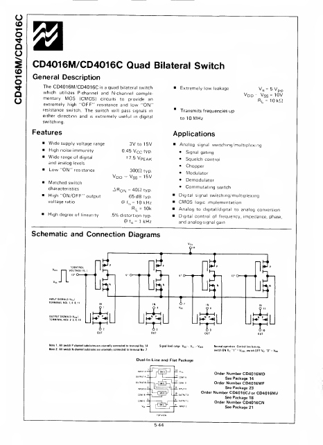
The CD4016M/CD4016C is a quad bilateral switch
Q which utilizes P-channel and N-channel ple-
O mentary MOS (CMOS) circuits to provide an extremely high "OFF" resistance and low "ON"
Extremely low leakage resistance switch. The switch will pass signals in
Transmits frequencies up either direction and is extremely useful in digital switchinq. to 10 MHz
V K = 5 V p_p
- V ss = 10V
R L = 10 k£2
Features
Wide supply voltage range High noise immunity Wide range of digital and analog levels
Low "ON" resistance
Matched switch characteristics
High "ON/OFF" output voltage ratio
High degree of linearity
3V to 15V 0.45 V cc typ.
±7.5Vpeak
3oon typ.
Vdd- V ss = 15V
-^R 0N = 4052 typ. 65 d B typ.
@f = 10 k Hz ls Ri 10k
.5% distortion typ.
@f, = s
1 k Hz
Applications
Analog signal switching/multiplexing
- Signal gating
- Squelch control
- Chopper
- Modulator
- Demodulator
- mutating switch
Digital signal switching/multiplexing
CMOS logic implementation
Analog to...