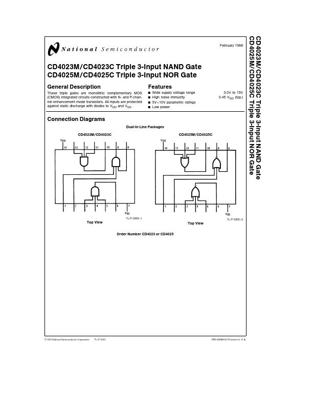
National Semiconductor CD4025C
The tables of ‘‘Recommended Operating Conditions’’ and ‘‘Electrical Characteristics’’ provide conditions for actual device operation Note 2 IDN and IDP are tested one output at a time 2 DC Electrical Characteristics CD4023C Symbol Parameter Conditions CD4025C Limits b 40 C a 25 C a 85 C Units Min IL PD VOL VOH II VNL VNH IDN IDP IDN IDP II Quiescent Device Current Quiescent Device Dissipation Package Output Voltage Low Level Output Voltage High Level Input Current Noise Immunity (All Inputs) Noise Immunity (All Inputs) VDD e 5 0V VO e 3 6V IO e 0A VDD e 10V VO e 7 2V IO e 0A VDD e 5 0V VO e 0...| Part No. | CD4025C |
|---|---|
| Datasheet | CD4025C Download |
| Manufacturer |  National Semiconductor |
| Description | Triple 3-Input NAND(NOR) Gate |
| Buy | Stock & Price |