CD4042BC Overview
Description
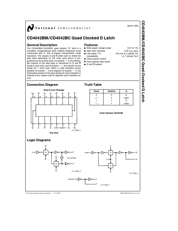
The CD4042BM CD4042BC quad clocked ‘‘D’’ latch is a monolithic complementary MOS (CMOS) integrated circuit constructed with P- and N-channel enhancement mode transistors The outputs Q and Q either latch or follow the data input depending on the clock level which is programmed by the polarity input For polarity e 0 the information present at the data input is transferred to Q and Q during 0 clock level and for polarity e 1 the transfer occurs during the 1 clock level When a clock transition occurs (positive for polarity e 0 and negative for polarity e 1) the information present at the input during the clock transition is retained at the outputs until an opposite clock transition occurs.