Datasheet Summary
CLC425 Ultra Low Noise Wideband Op Amp
June 1999
CLC425 Ultra Low Noise Wideband Op Amp
General Description
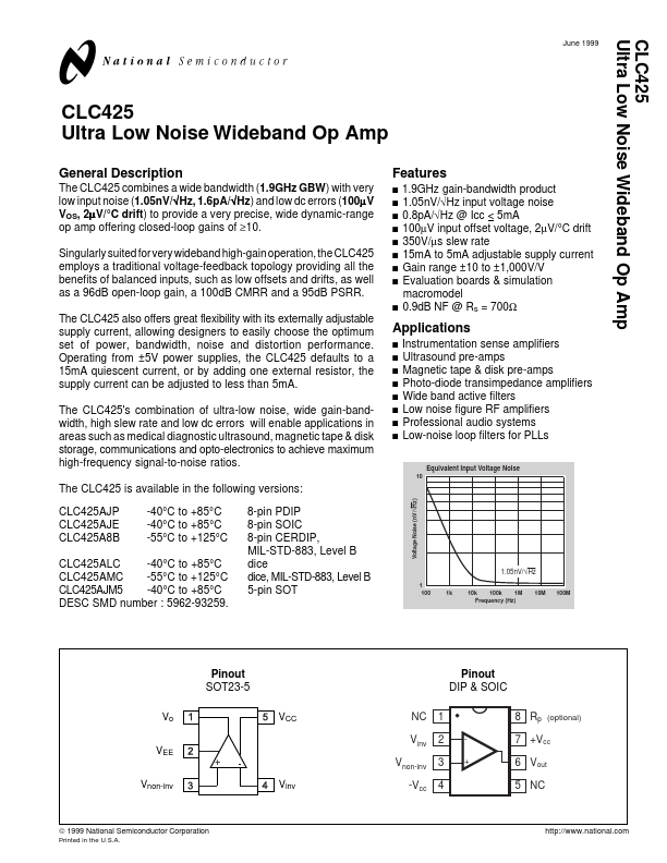
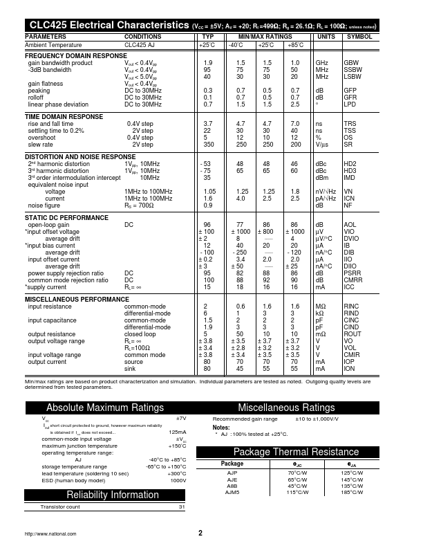
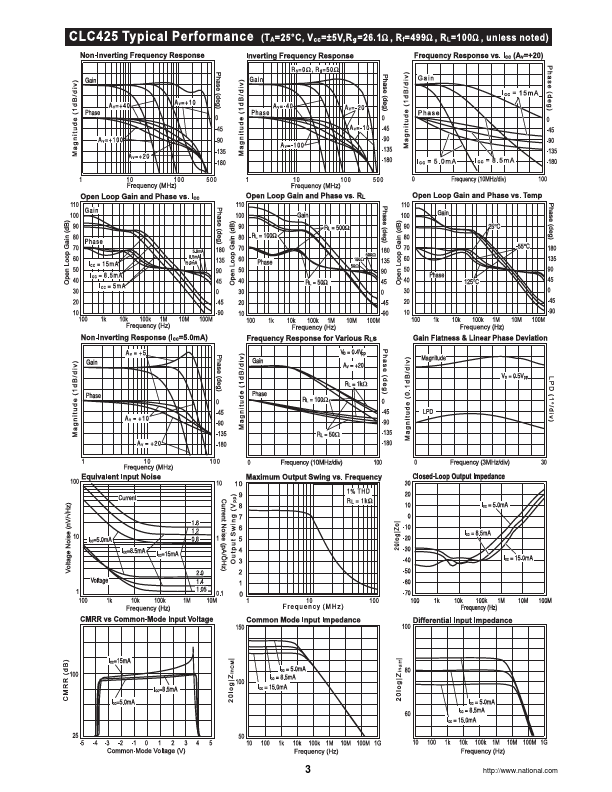
The CLC425 bines a wide bandwidth (1.9GHz GBW) with very low input noise (1.05nV/√ Hz, 1.6pA/√ Hz) and low dc errors (100µ V VOS, 2µ V/°C drift) to provide a very precise, wide dynamic-range op amp offering closed-loop gains of ≥10. Singularly suited for very wideband high-gain operation, the CLC425 employs a traditional voltage-feedback topology providing all the benefits of balanced inputs, such as low offsets and drifts, as well as a 96dB open-loop gain, a 100dB CMRR and a 95dB PSRR. The CLC425 also offers great flexibility with its externally adjustable supply current,...