Datasheet Summary
CLC501 High-Speed Output Clamping Op Amp
June 1999
CLC501 High-Speed Output Clamping Op Amp
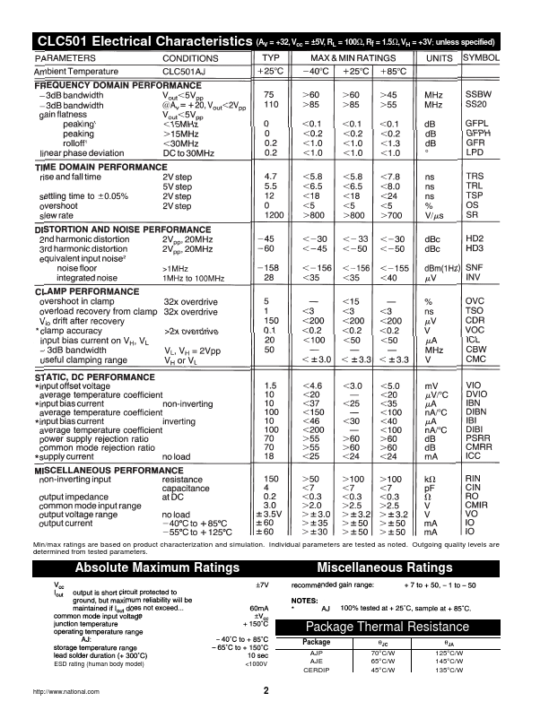
General Description Features s s s s s
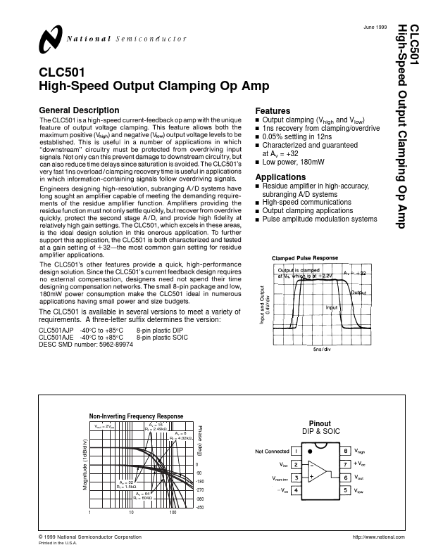
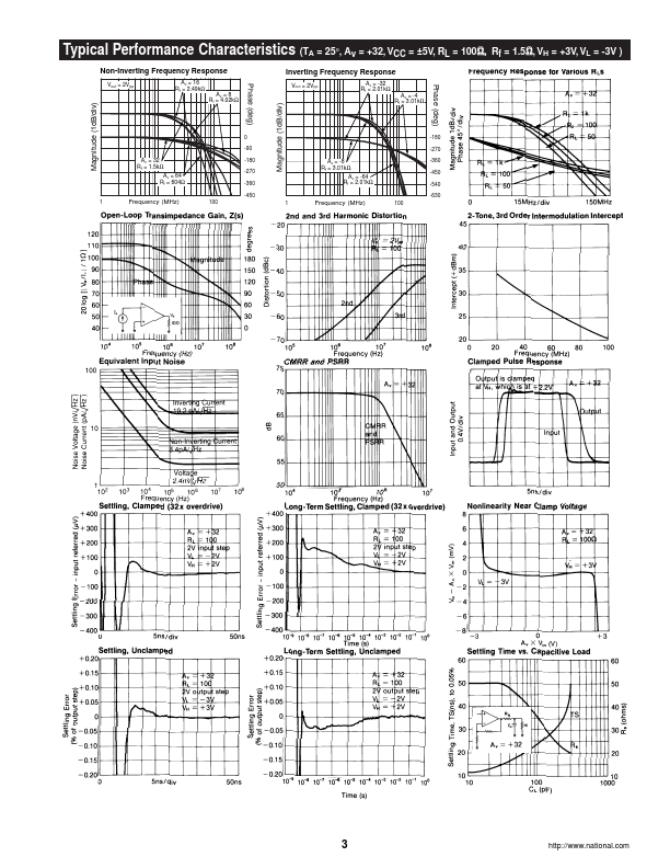
Output clamping (Vhigh and Vlow) 1ns recovery from clamping/overdrive 0.05% settling in 12ns Characterized and guaranteed at Av = +32 Low power, 180mW Residue amplifier in high-accuracy, subranging A/D systems High-speed munications Output clamping applications Pulse amplitude modulation systems
Applications s s s s
The CLC501 is available in several versions to meet a variety of requirements. A three-letter suffix determines the version:
CLC501AJP -40°C to +85°C 8-pin plastic DIP CLC501AJE -40°C to +85°C 8-pin plastic SOIC DESC SMD number:...