Description
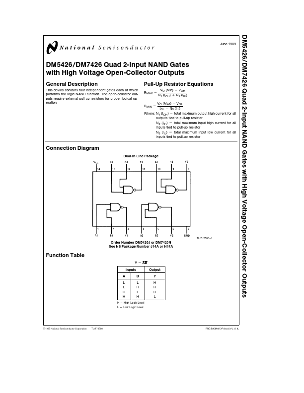
This device contains four independent gates each of which performs the logic NAND function The open-collector outputs require external pull-up resistors for proper logical operation Pull-Up Resistor Equations RMAX e VO (Min) b VOH N1 (IOH) a N2 (IIH) RMIN e VO (Max) b VOL IOL b N3 (IIL) Where N1 (IOH) e total maximum output high current for all outputs tied to pull-up resistor N2 (IIH) e total maximum input high current for all inputs tied to pull-up resistor N3 (IIL) e total maximum input low current for all inputs tied to pull-up resistor Connection Diagram Dual-In-Line Package Function Table Order Number DM5426J or DM7426N See NS Package Number J14A or N14A Y e AB Inputs Output AB Y LL LH HL HH H H H L H e High Logic Level L e Low Logic Level C1995 National Semiconductor C.