Description
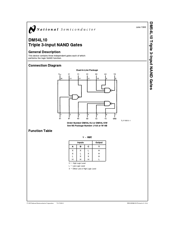
This device contains three independent gates each of which performs the logic NAND function Connection Diagram Dual-In-Line Package TL F 6619 - 1 Order Number DM54L10J or DM54L10W See NS Package Number J14A or W14B Function Table Y e ABC Inputs A X X L H B X L X H C L X X H Output Y H H H L H e High Logic Level L e Low Logic Level X e Either Low or High Logic Level C1995 National Semiconductor Corporation TL F 6619 RRD-B30M105 Printed in U S A If Military Aerospace specified devices are required please contact the National Semiconductor Sales Office Distributors for availability and specifications Supply Voltage 8V Input Voltage 5 5V Operating Free Air Temperature Range b 55 C to a 125 C DM54L b 65 C to a 150 C Storage Temperature Range Note The ‘‘ Remended Operating Conditions Symbol VCC VIH VIL IOH IOL TA Parameter Min Supply Voltage High Level Input Voltage Low Level Input Voltage High Level Output Current Low Level Output Current Free Air Operating Temperature b 55 DM54L10 Nom 5 Max 55 Units V V 07 b0 2 45 2 V mA mA C 2 125 Symbol VOH VOL II IIH IIL IOS ICCH ICCL Parameter High Level Output Voltage Low Level Output Voltage Input Current Input Voltage Max Conditions VCC e Min IOH e Max VIL e Max VCC e Min IOL e Max VIH e Min VCC e Max VI e 5 5V VCC e Max VI e 2 4V VCC e Max VI e 0 3V VCC e Max (Note 2) VCC e Max VCC e Max Min 24 Typ (Note 1) 33 0 15 03 01 10 b 0 18 b3 b 15 Max Units V V mA mA mA mA mA mA High Level Input Current Low Level Input Current Short Circuit Output Current Supply Current with Outputs High Supply Current with Outputs Low 0 33 0 87 06 1 53 Switching Characteristics at VCC e 5V and TA e 25 C (See Section 1 for Test Waveforms and Output Load) Symbol tPLH tPHL Parameter Propagation Delay Time Low to High Level Output Propagation Delay Time High to Low Level Output Conditions RL e 4 kX CL e 50 pF Min Max 60 60 Units ns ns Note 1 All typicals are at VCC e 5V TA e 25 C Note 2 Not more than one output should be shorted at a time 2 Physical Dimensions inches (millimeters) 14-Lead Ceramic Dual-In-Line Package (J) Order Number DM54L10J NS Package Number J14A 3 DM54L10 Triple 3-Input NAND Gates Physical Dimensions inches (millimeters) (Continued) 14-Lead Ceramic Flat Package (W) Order Number DM54L10W NS Package Number W14B LIFE SUPPORT POLICY NATIONAL’S PRODUCTS ARE NOT AUTHORIZED FOR USE AS CRITICAL PONENTS IN LIFE SUPPORT DEVICES OR SYSTEMS WITHOUT THE EXPRESS WRITTEN APPROVAL OF THE PRESIDENT OF NATIONAL SEMICONDUCTOR CORPORATION As used herein 1 Life support devices or systems are devices or systems which (a) are intended for surgical implant into the body or (b) support or sustain life and whose failure to perform when properly used in accordance with instructions for use provided in the labeling can be reasonably expected to result in a significant injury to the user National Semiconductor Corporation 1111 West Bardin Road Arlington TX 76017 Tel 1(800) 272-9959 Fax 1(800) 737-7018 2 A critical ponent is any ponent of a life support device or system whose failure to perform can be reasonably expected to cause the failure of the life support device or system or to affect its safety or effectiveness National Semiconductor Europe Fax (a49) 0-180-530 85 86 Email cnjwge tevm2 nsc Deutsch Tel (a49) 0-180-530 85 85 English Tel (a49) 0-180-532 78 32 Fran ais Tel (a49).