Description
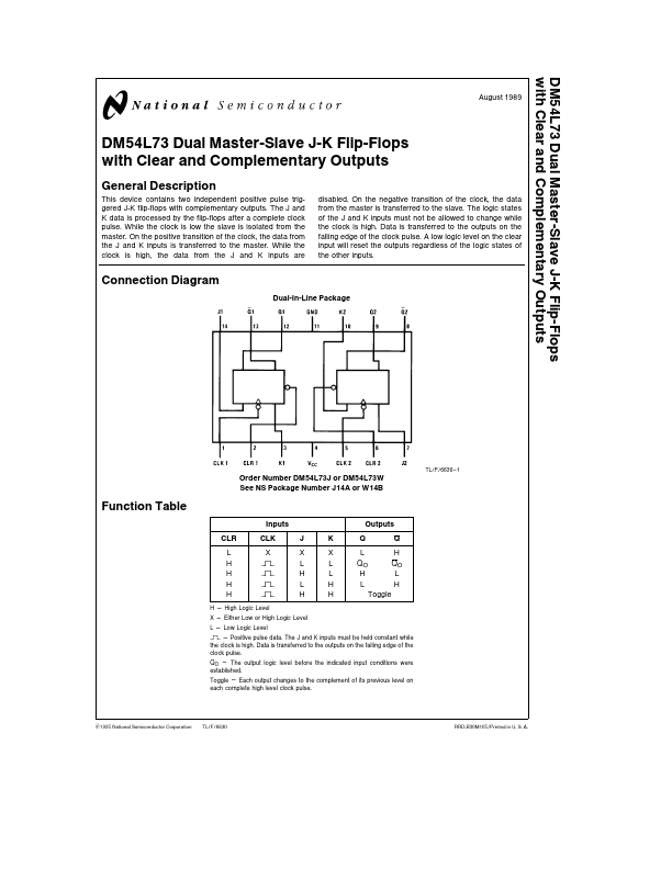
This device contains two independent positive pulse triggered J-K flip-flops with plementary outputs The J and K data is processed by the flip-flops after a plete clock pulse While the clock is low the slave is isolated from the master On the positive transition of the clock the data from the J and K inputs is transferred to the master While the clock is high the data from the J and K inputs are disabled On the negative transition of the clock the data from the master is transferred to the slave The logic states of the J and K inputs must not be allowed to change while the clock is high Data is transferred to the outputs on the falling edge of the clock pulse A low logic level on the clear input will reset the outputs regardless of the logic states of the other inputs Connection Diagram Dual-In-Line Package TL F 6630 - 1 Order Number DM54L73J or DM54L73W See NS Package Number J14A or W14B Function Table Inputs CLR L H H H H CLK X J X L H L H K X L L H H Outputs Q Q L H QO QO H L L H Toggle H e High Logic Level X e Either Low or High Logic Level L e Low Logic Level e Positive pulse data The J and K inputs must be held constant while the clock is high Data is transferred to the outputs on the falling edge of the clock pulse QO e The output logic level before the indicated input conditions were established Toggle e Each output changes to the plement of its previous level on each plete high level clock pulse C1995 National Semiconductor Corporation TL F 6630 RRD-B30M105 Printed in U S A If Military Aerospace specified devices are required please contact the National Semiconductor Sales Office Distributors for availability and specifications Supply Voltage Input Voltage Storage Temperature Range 8V 5 5V Note The ‘‘ b 65 C to a 150 C Operating Free Air Temperature Range b 55 C to a 125 C DM54L Remended Operating Conditions Symbol VCC VIH VIL Supply Voltage High Level Input Voltage Low Level Input Voltage Clock Others IOH IOL fCLK tW High Level Output Current Low Level Output Current Clock Frequency (Note 2) Pulse Width (Note 2) Clock High Clock Low Clear Low tSU tH TA Note 1 The symbols ( Parameter Min 45 2 DM54L73 Nom 5 Max 55 Units V V 06 07 b0 2 V mA mA MHz 2 0 100 100 100 0u 0v b 55 6 ns Input Setup Time (Notes 1 Input Hold Time (Notes 1 2) 2) ns ns 125 C Free Air Operating Temperature u v) indicate the edge of the clock pulse used for reference u for rising edge v for falling edge Note 2 TA e 25 C and VCC e 5V 2 Symbol VOH VOL II Parameter High Level Output Voltage Low Level Voltage Voltage Input Current Input Voltage Max Conditions VCC e Min IOH e Max VIL e Max VIH e Min VCC e Min IOL e Max VIL e Max VIH e Min VCC e Max VI e 5 5V J K Clear Clock IIH High Level Input Current VCC e Max VI e 2 4V J K Clear Clock IIL Low Level Input Current VCC e Max VI e 0 3V J K Clear Clock IOS ICC Short Circuit Output Current Supply Current VCC e Max VCC e Max (Note 2) b3 Min 24 Typ (Note 1) 33 0 15 Max Units V 03 100 200 200 10 20 b 200 b 0 18 b 0 36 b 0 36 b 15 V mA mA mA mA mA 15 2 88 Note 1 All typicals are at VCC e 5V TA e 25 C Note 2 With all outputs open ICC is measured with the Q and Q outputs high in turn At the time of measurement the clock is grounded Switching Characteristics VCC e 5V and.