Description
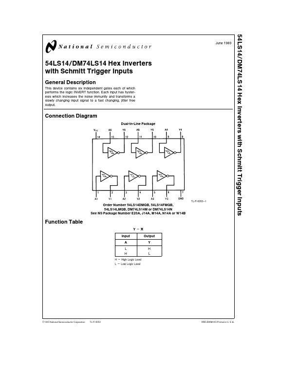
This device contains six independent gates each of which performs the logic INVERT function Each input has hysteresis which increases the noise immunity and transforms a slowly changing input signal to a fast changing jitter free output Connection Diagram Dual-In-Line Package TL F 6353 - 1 Order Number 54LS14DMQB 54LS14FMQB 54LS14LMQB DM74LS14M or DM74LS14N See NS Package Number E20A J14A M14A N14A or W14B Function Table YeA Input A L H H e High Logic Level L e Low Logic Level Output Y H L C1995 National Semiconductor Corporation TL F 6353 RRD-B30M105 Printed in U S A Supply Voltage 7V Input Voltage 7V Operating Free Air Temperature Range b 55 C to a 125 C 54LS DM74LS 0 C to a 70 C Storage Temperature Range b 65 C to a 150 C Note The ‘‘ Remended Operating Conditions Symbol VCC VT a VTb HYS IOH IOL TA Parameter Min Supply Voltage Positive-Going Input Threshold Voltage (Note 1) Negative-Going Input Threshold Voltage (Note 1) Input Hysteresis (Note 1) High Level Output Current Low Level Output Current Free Air Operating Temperature b 55 54LS14 Nom 5 16 08 08 b0 4 DM74LS14 Max 55 20 11 Min 4 75 14 05 04 Nom 5 16 08 08 b0 4 Units Max 5 25 19 1 V V V V mA mA C 45 15 06 04 4 125 0 8 70 Symbol VI VOH Parameter Input Clamp Voltage High Level Output Voltage Low Level Output Voltage Conditions VCC e Min II e b18 mA VCC e Min IOH e Max VIL e Max VCC e Min IOL e Max VIH e Min VCC e Min IOL e 4 mA IT a IT b II Input Current at Positive-Going Threshold Input Current at Negative-Going Threshold Input Current Input Voltage Max VCC e 5V VI e VT a VCC e 5V VI e VTb VCC e Max VI e 7V VCC e Max VI e 10 0V VCC e Max VI e 2 7V VCC e Max VI e 0 4V VCC e Max (Note 3) VCC e Max VCC e Max 54LS DM74 b 20 b 20 Min Typ (Note 2) Max b1 5 Units V V 54LS DM74 54LS DM74 DM74 DM74 DM74 DM74 54LS 25 27 34 34 0 25 0 35 0 25 b 0 14 b 0 18 VOL 04 05 04 mA mA 01 20 b0 4 b 100 b 100 V mA mA mA mA IIH IIL IOS High Level Input Current Low Level Input Current Short Circuit Output Current Supply Current with Outputs High Supply Current with Outputs Low ICCH ICCL 86 12 16 21 mA mA Note 1 VCC e 5V Note 2 All typicals are at VCC e 5V TA e 25 C Note 3 Not more than one output should be shorted at a time and the duration should not exceed one second 2 Switching Characteristics at VCC e 5V and TA e 25 C (See Section 1 for Test Waveforms and Output Load) RL e 2 k X Symbol Parameter Min tPLH tPHL Propagation Delay Time Low to High Level Output Propagation Delay Time High to Low Level Output 5 5 CL e 15 pF Max 22 22 CL e 50 pF Min 8 10 Max 25 33 ns ns Units 3 Physical Dimensions inches (millimeters) Ceramic Leadless Chip Carrier (E) Order Number 54LS14LMQB NS Package Number E20A 14-Lead Ceramic Dual-In-Line Package (J) Order Number 54LS14DMQB NS Package Number J14A 4 Physical Dimensions inches (millimeters) (Continued) 14-Lead Small Outline Molded Package (M) Order Number DM74LS14M NS Package Number M14A 14-Lead Molded Dual-In-Line Package (N) Order Number DM74LS14N NS Package Number N14A 5 54LS14 DM74LS14 Hex Inverters with Schmitt Trigger Inputs Physical Dimensions inches (millimeters) (Continued) 14-Lead Ceramic Flat P.