DM54LS279
Description
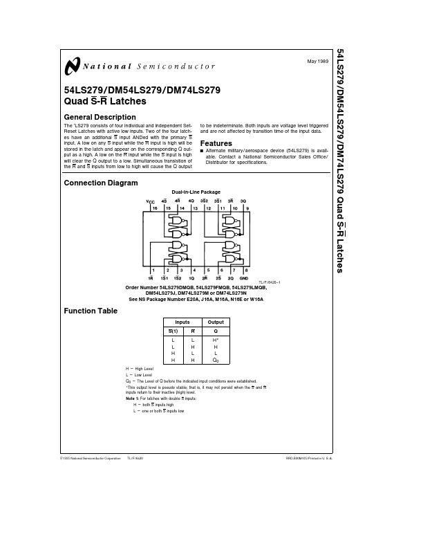
The ’LS279 consists of four individual and independent SetReset Latches with active low inputs Two of the four latches have an additonal S input ANDed with the primary S input A low on any S input while the R input is high will be stored in the latch and appear on the corresponding Q output as a high A low on the R input while the S input is high will clear the Q output to a low Simultaneous transistion of the R and S inputs from low to high will cause the Q output to be indeterminate Both inputs are voltage level triggered and are not affected by transition time of the input data.