DM7497 Overview
Key Specifications
Package: DIP
Operating Voltage: 5 V
Max Voltage (typical range): 5.25 V
Min Voltage (typical range): 4.75 V
Description
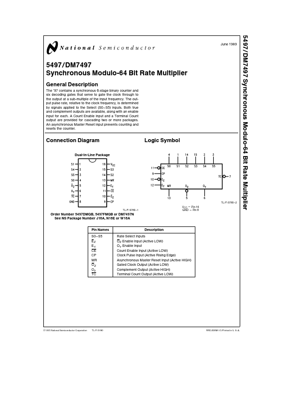
The ’97 contains a synchronous 6-stage binary counter and six decoding gates that serve to gate the clock through to the output at a sub-multiple of the input frequency The output pulse rate relative to the clock frequency is determined by signals applied to the Select (S0–S5) inputs Both true and complement outputs are available along with an enable input for each A Count Enable input and a Terminal Count output are provided for cascading two or more packages An asynchronous Master Reset input prevents counting and resets the counter Connection Diagram Dual-In-Line Package Logic Symbol TL F 9780 – 2 TL F 9780 – 1 VCC e Pin 16 GND e Pin 8 Order Number 5497DMQB 5497FMQB or DM7497N See NS Package Number J16A N16E or W16A Pin Names S0–S5 EZ EY CE CP MR OZ Oy TC Description Rate Select Inputs OZ Enable Input (Active LOW) OY Enable Input Count Enable Input (Active LOW) Clock Pulse Input (Active Rising Edge) Asynchronous Master Reset Input (Active HIGH) Gated Clock Output (Active LOW) Complement Output (Active HIGH) Terminal Count Output (Active LOW) C1995 National Semiconductor Corporation TL F 9780 RRD-B30M115 Printed in U S A If Military Aerospace specified devices are required please contact the National Semiconductor Sales Office Distributors for availability and specifications Supply Voltage 7V Input Voltage 5 5V Operating Free Air Temperature Range b 55 C to a 125 C 54 DM74 0 C to a 70 C b 65 C to a 150 C Storage Temperature Range Note The ‘‘.