Description
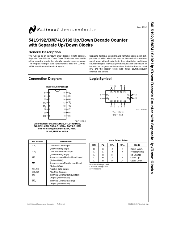
The ’LS192 is an up down BCD decade (8421) counter Separate Count Up and Count Down Clocks are used and in either counting mode the circuits operate synchronously The outputs change state synchronous with the LOW-toHIGH transitions on the clock inputs Separate Terminal Count Up and Terminal Count Down outputs are provided which are used as the clocks for a subsequent stage without extra logic thus simplifying multistage counter designs Individual preset inputs allow the circuits to be used as programmable counters Both the Parallel Load (PL) and the Master Reset (MR) inputs asynchronously override the clocks Connection Diagram Dual-In-Line Package Logic Symbol TL F 10178 - 2 VCC e Pin 16 GND e Pin 8 TL F 10178 - 1 Order Number 54LS192DMQB 54LS192FMQB 54LS192LMQB DM74LS192M or DM74LS192N See NS Package Number E20A J16A M16A N16E or W16A Pin Names CPU CPD MR PL P0 - P3 Q0 - Q3 TCD TCU Description Count Up Clock Input (Active Rising Edge) Count Down Clock Input (Active Rising Edge) Asynchronous Master Reset Input (Active HIGH) Asynchronous Parallel Load Input (Active LOW) Parallel Data Inputs Flip-Flop Outputs Terminal Count Down (Borrow) Output (Active LOW) Terminal Count Up (Carry) Output (Active LOW) MR H L L L L PL X L H H H Mode Select Table CPU X X H L H CPD X X H H L Mode Reset (Asyn ) Preset (Asyn ) No Change Count Up Count Down H e HIGH Voltage Level L e LOW Voltage Level X e Immaterial C1995 National Semiconductor Corporation TL F 10178 RRD-B30M105 Printed in U S A If Military Aerospace specified devices are required please contact the National Semiconductor Sales Office Distributors for availability and specifications Supply Voltage 7V Input Voltage 7V Operating Free Air Temperature Range b 55 C to a 125 C 54LS DM74LS 0 C to a 70 C Storage Temperature Range b 65 C to a 150 C Note The ‘‘ Remended Operating Conditions Symbol VCC VIH VIL IOH IOL TA ts (H) ts (L) th (H) th (L) tw (L) tw (L) tw (H) trec trec Parameter Min Supply Voltage High Level Input Voltage Low Level Input Voltage High Level Output Voltage Low Level Output Current Free Air Operating Temperature Setup Time HIGH or LOW Pn to PL Hold Time HIGH or LOW Pn to PL CP Pulse Width LOW PL Pulse Width LOW MR Pulse Width HIGH Recovery Time MR to CP Recovery Time PL to CP b 55 54LS192 Nom 5 Max 55 Min 4 75 2 07 b0 4 DM74LS192 Nom 5 Max 5 25 Units V V 08 b0 4 45 2 V mA mA C ns ns ns ns ns ns ns 4 125 0 20 10 3 3 17 20 15 3 10 8 70 20 20 3 3 17 20 15 3 10 Symbol VI VOH Parameter Input Clamp Voltage High Level Output Voltage Conditions VCC e Min II e b18 mA VCC e Min IOH e Max VIL e Max VCC e Min IOL e Max VIH e Min IOL e 4 mA VCC e Min II Input Current Input Voltage Max VCC e Max VI e 10V VI e 7V VCC e Max VI e 2 7V VCC e Max VI e 0 4V VCC e Max (Note 2) VCC e Max MR PL e GND Other Inputs e 4 5V 54LS DM74 b 20 b 20 Min Typ (Note 1) Max b1 5 Units V V 54LS DM74 54LS DM74 DM74 DM54 DM74 25 27 04 05 04 01 20 b0 4 b 100 b 100 VOL Low Level Output Voltage V mA mA mA mA IIH IIL IOS High Level Input Current Low Level Input Current Short Circuit Output Current Supply Current ICC 31 mA Note 1 All typicals are at VCC e 5V TA e 25 C Note 2 Not more than one output should be shorted at a time and the duration should not exceed one second 2 Switching Characteris.