DM74LS367A
Description
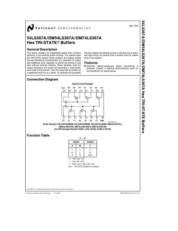
This device contains six independent gates each of which performs a non-inverting buffer function The outputs have the TRI-STATE feature
When enabled the outputs exhibit the low impedance characteristics of a standard LS output with additional drive capability to permit the driving of bus lines without external resistors When disabled both the output transistors are turned off presenting a high-impedance state to the bus line Thus the output will act neither as a significant load nor as a driver To minimize the possibility that two outputs will attempt to take a mon bus to opposite logic levels the disable time is shorter than the enable time of the outputs
Features
Y Alternate military aerospace device (54LS367A) is available Contact a National Semiconductor sales office distributor for specifications
Connection Diagram
Dual-In-Line Package
TL F 6429
- 1
Order Number 54LS367ADMQB 54LS367AFMQB 54LS367ALMQB DM54LS367AJ DM54LS367AW DM74LS367AM or DM74LS367AN
See NS...