Description
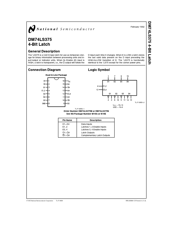
The ’LS375 is a 4-bit D-type latch for use as temporary storage for binary information between processing units and input output or indicator units When its Enable (E) input is HIGH a latch is transparent i e the Q output will follow the D input each time it changes When E is LOW a latch stores the last valid data present on the D input preceding the HIGH-to-LOW transition of E The ’LS375 is functionally identical to the ’LS75 except for the corner power pins Connection Diagram Dual-In-Line Package Logic Symbol TL F 9830 - 2 TL F 9830 - 1 VCC e Pin 16 GND e Pin 8 Order Number DM74LS375M or DM74LS375N See NS Package Number M16A or N16E Pin Name D1-D4 E1 2 E3 4 Q1-Q4 Q1-Q4 Description Data Inputs Latches 1 2 Enable Inputs Latches 3 4 Enable Inputs Latch Outputs plementary Latch Outputs C1995 National Semiconductor Corporation TL F 9830 RRD-B30M115 Printed in U S A Supply Voltage Input Voltage Operating Free Air Temperature Range Storage Temperature Range 7V 7V 0 C to a 70 C b 65 C to a 150 C Note The ‘‘ Remended Operating Conditions Symbol VCC VIH VIL IOH IOL TA ts (H) ts (L) th (H) th (L) tw (H) Parameter Supply Voltage High Level Input Voltage Low Level Input Voltage High Level Output Current Low Level Output Current Free Air Operating Temperature Setup Time HIGH or LOW Dn to En Hold Time HIGH or LOW Dn to En En Pulse Width HIGH 0 20 0 20 Min 4 75 2 08 b0 4 Nom 5 Max 5 25 Units V V V mA mA C ns ns ns 8 70 Over remended operating free air temperature range (unless otherwise noted) Symbol VI VOH VOL Parameter Input Clamp Voltage High Level Output Voltage Low Level Output Voltage Conditions VCC e Min II e b18 mA VCC e Min IOH e Max VIL e Max VCC e Min IOL e Max VIH e Min IOL e 4 mA VCC e Min II Input Current Input Voltage Max VCC e Max VI e 7V Others Enable Input VCC e Max VI e 2 7V Others Enable Input IIL Low Level Input Current VCC e Max VI e 0 4V Others Enable Input IOS ICC Short Circuit Output Current Supply Current VCC e Max (Note 2) VCC e Max b 20 Min Typ (Note 1) Max b1 5 Units V V 27 34 0 35 0 25 05 04 01 04 20 80 b0 4 b1 2 b 100 V mA mA mA mA mA mA mA mA IIH High Level Input Current 12 Note 1 All typicals are at VCC e 5V TA e 25 C Note 2 Not more than one output should be shorted at a time and the duration should not exceed one second 2 Switching Characteristics VCC e a 5 0V TA e a 25 C Symbol tPLH tPHL tPLH tPHL tPLH tPHL tPLH tPHL Parameter Min Propagation Delay Dn to Qn Propagation Delay Dn to Qn Propagation Delay En to Qn Propagation Delay En to Qn CL e 15 pF Max 27 23 20 15 27 25 30 18 ns ns ns ns Units Truth Table (Each Latch) tn D H L tn e Bit time before Enable negative going transition tn a 1 e Bit time after Enable negative going transition H e HIGH Voltage Level L e LOW Voltage Level tn a 1 Q H L Logic Diagram (1 4 of diagram shown) TL F 9830 - 3 3 4 Physical Dimensions inches (millimeters) 16-Lead Small Outline Molded Package (M) Order Number DM74LS375M NS Package Number M16A 5 DM74LS375 4-Bit Latch Physical Dimensions inches (millimeters) (Continued) 16-Lead Molded Dual-In-Line Package (N) Order Number DM74LS375N NS Package Number N16E LIFE SUPPORT POLICY NATIONAL’S PRODUCTS ARE NOT AUTHORIZED FOR USE AS CRITICAL PONENTS IN LIFE SUPPORT DEVICES OR SYSTEMS WITHOUT THE EXPRESS WRITTEN APPROVAL OF THE PRESIDENT OF NATIONAL SEMICONDUCTOR CORPORATION As used herein 1 Life support devices or systems are devices or systems which (a) are intended for surg.