DM74LS40
DM74LS40 is Dual 4-Input NAND Buffer manufactured by National Semiconductor.
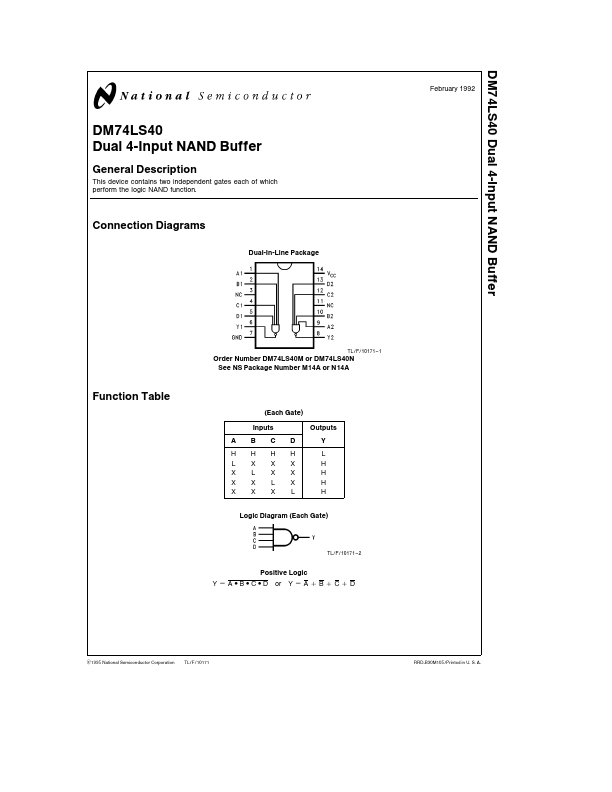
Description
This device contains two independent gates each of which perform the logic NAND function
Connection Diagrams
Dual-In-Line Package
TL F 10171
- 1
Order Number DM74LS40M or DM74LS40N See NS Package Number M14A or N14A
Function Table
(Each Gate) Inputs A H L X X X B H X L X X C H X X L X D H X X X L Outputs Y L H H H H
Logic Diagram (Each Gate)
TL F 10171
- 2
Positive Logic Y e A B C D or Y e A a B a C a D
C1995 National Semiconductor Corporation
TL F 10171
RRD-B30M105 Printed in U S A
Absolute Maximum Ratings (Note)
Supply Voltage Input Voltage Operating Free Air Temperature Range DM74LS Storage Temperature Range 7V 7V 0 C to a 70 C b 65 C to a 150 C
Note The ‘‘Absolute Maximum Ratings’’ are those values beyond which the safety of the device cannot be guaranteed The device should not be operated at these limits The parametric values defined in the ‘‘Electrical Characteristics’’ table are not guaranteed at the absolute maximum ratings The ‘‘Remended Operating Conditions’’ table will define the conditions for actual device operation
Remended Operating Conditions
Symbol VCC VIH VIL IOH IOL TA Parameter Min Supply Voltage High Level Input Voltage Low Level Input Voltage High Level Output Current Low Level Output Current Free Air Operating Temperature 0 4 75 2 08 b1 2
DM74LS40 Nom 5 Max 5 25
Units V V V m A m A C
24 70
Electrical Characteristics over remended operating free air temperature range (unless otherwise noted)
Symbol VI VOH VOL Parameter Input Clamp Voltage High Level Output Voltage Low Level Output Voltage Conditions VCC e Min II e b18 m A VCC e Min IOH e Max VIL e Max VCC e Min IOL e Max VIH e Min IOL e 12 m A VCC e Min II IIH IIL IOS ICCH ICCL Input Current Input Voltage Max VCC e Max VI e 7V VCC e Max VI e 2 7V VCC e Max VI e 0 4V VCC e Max (Note 2) VCC e Max VIN e GND VCC e Max VIN e OPEN b 30
Min
Typ (Note 1)
Max b1 5
Units V V
27 05 04 01 20 b0 4 b 130
V m A m A m A m A m A m A
High Level Input Current Low Level Input...