DS64EV100
DS64EV100 is Programmable Single Equalizer manufactured by National Semiconductor.
DS64EV100 Programmable Single Equalizer
..
November 9, 2007
DS64EV100 Programmable Single Equalizer
General Description
The DS64EV100 programmable equalizer provides pensation for transmission medium losses and reduces the medium-induced deterministic jitter for NRZ data channel. The DS64EV100 is optimized for operation up to 10 Gbps for both cables and FR4 traces. The equalizer channel has eight levels of input equalization that can be programmed by three control pins. The equalizer supports both AC and DC-coupled data paths for long run length data patterns such as PRBS-31, and balanced codes such as 8b/10b. The device uses differential current-mode logic (CML) inputs and outputs, and is available in a 3 mm x 4 mm 14-pin leadless LLP package. Power is supplied from either a 2.5V or 3.3V supply.
Features
- -
- -
- -
- -
- -
- -
Equalizes up to 24 d B loss at 10 Gbps Equalizes up to 22 d B loss at 6.4 Gbps 8 levels of programmable equalization Operates up to 10 Gbps with 30” FR4 traces Operates up to 6.4 Gbps with 40” FR4 traces 0.175 UI residual deterministic jitter at 6.4 Gbps with 40” FR4 traces Single 2.5V or 3.3V power supply Supports AC or DC-Coupling with wide input monmode Low power consumption: 100 m W Typ at 2.5V Small 3 mm x 4 mm 14-pin LLP package >8 k V HBM ESD -40 to 85°C operating temperature range
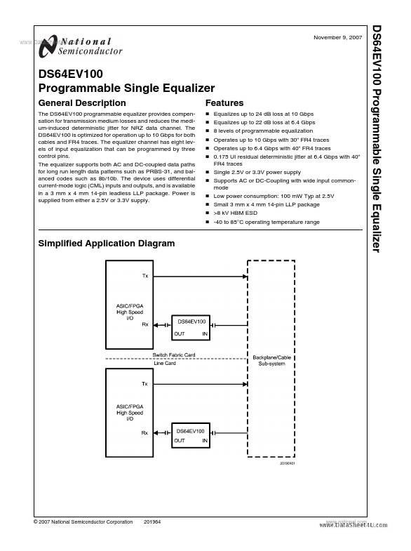
Simplified Application Diagram
© 2007 National Semiconductor Corporation
.national.
..
Pin Diagram
Top View 3mm x 4mm 14-Pin LLP Package Order number DS64EV100 See NS Package Number SDA14A
Pin Descriptions
Pin Name Pin Number I/O, Type I, CML Description
HIGH SPEED DIFFERENTIAL I/O IN+ IN- OUT+ OUT- BST_2 BST_1 BST_0 POWER VDD GND Exposed Pad OTHER NC 1 Reserved. Do not connect. 5 2, 6, 9, 10, 13 PAD I, Power VDD = 2.5V ±5% or 3.3V ±10%. VDD pins should be tied to VDD plane through low inductance path. A 0.01μF bypass capacitor should be connected between each VDD...