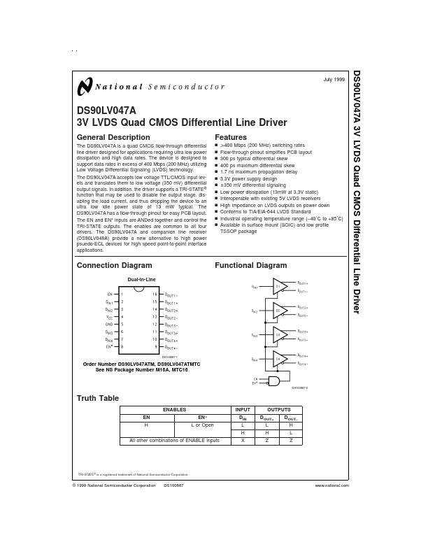
Datasheet4U Logo Datasheet4U.com

DS90LV047A - 3V LVDS Quad CMOS Differential Line Driver

Datasheet Summary

Description

The DS90LV047A is a quad CMOS flow-through differential line driver designed for applications requiring ultra low power dissipation and high data rates.

The device is designed to support data rates in excess of 400 Mbps (200 MHz) utilizing Low Voltage Differential Signaling (LVDS) technology.

Features

  • n n n n n n n n n n n n n > 400 Mbps (200 MHz) switching rates Flow-through pinout simplifies PCB layout 300 ps typical differential skew 400 ps maximum differential skew 1.7 ns maximum propagation delay 3.3V power supply design ± 350 mV differential signaling Low power dissipation (13mW at 3.3V static) Interoperable with existing 5V LVDS receivers High impedance on LVDS outputs on power down Conforms to TIA/EIA-644 LVDS Standard Industrial operating temperature range (.
  • 40˚C to +85˚C) A.

📥 Download Datasheet

Datasheet preview – DS90LV047A

Datasheet Details

Part number DS90LV047A
Manufacturer National Semiconductor
File Size 268.11 KB
Description 3V LVDS Quad CMOS Differential Line Driver
Datasheet download datasheet DS90LV047A Datasheet
Additional preview pages of the DS90LV047A datasheet.
Other Datasheets by National Semiconductor

Full PDF Text Transcription

Click to expand full text
DS90LV047A 3V LVDS Quad CMOS Differential Line Driver July 1999 DS90LV047A 3V LVDS Quad CMOS Differential Line Driver General Description The DS90LV047A is a quad CMOS flow-through differential line driver designed for applications requiring ultra low power dissipation and high data rates. The device is designed to support data rates in excess of 400 Mbps (200 MHz) utilizing Low Voltage Differential Signaling (LVDS) technology. The DS90LV047A accepts low voltage TTL/CMOS input levels and translates them to low voltage (350 mV) differential output signals. In addition, the driver supports a TRI-STATE ® function that may be used to disable the output stage, disabling the load current, and thus dropping the device to an ultra low idle power state of 13 mW typical.
Published: |