LM1391
Overview
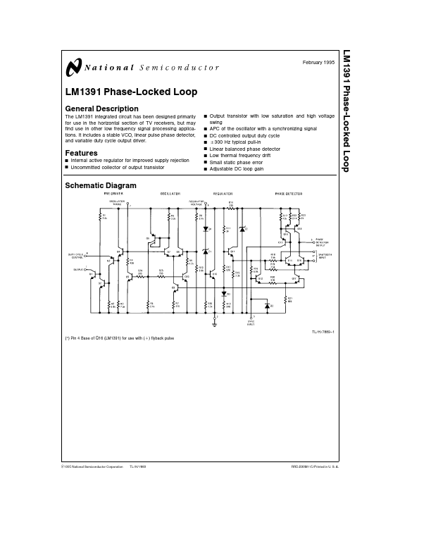
The LM1391 integrated circuit has been designed primarily for use in the horizontal section of TV receivers but may find use in other low frequency signal processing applications It includes a stable VCO linear pulse phase detector and variable duty cycle output driver Y Y Y Y Y.