GENERAL DESCRIPTION
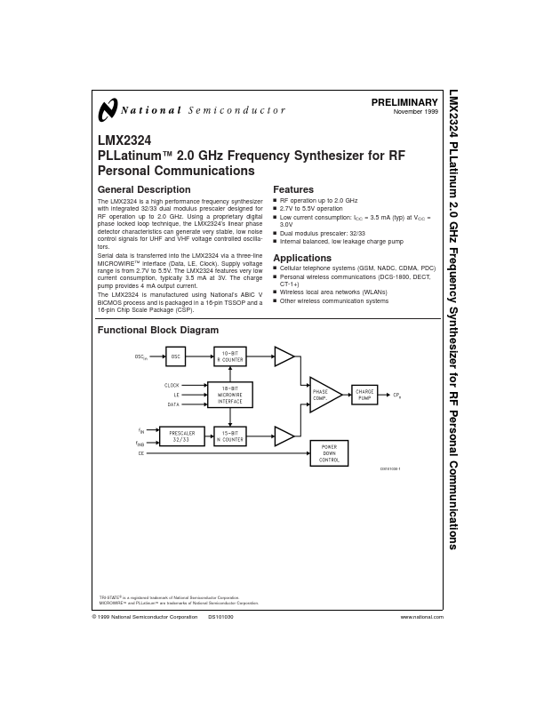
Using a proprietary digital phase locked loop technique, the LMX2324’s linear phase detector characteristics can generate very stable, low noise control signals for UHF and VHF voltage controlled oscillators. Serial data is transferred into the LMX2324 via a three-line MICROWIRE™ interface (Data, LE, Clock). Supply voltage range is from 2.7V to 5.5V. The charge pump provides 4 mA output current. The LMX2324 is manufactured using National’s ABiC V BiCMOS process and is packaged in a 16-pin TSSOP and a 16-pin Chip Scale Package (CSP). FEATURES
n RF operation up to 2.0 GHz n 2.7V to 5.5V operation n Low current consumption: ICC = 3.5 mA (typ) at VCC = 3.0V n Dual modulus prescaler: 32/33 n Internal balanced, low leakage charge pump APPLICATIONS
n Cellular telephone systems (GSM, NADC, CDMA, PDC) n Personal wireless communications (DCS-1800, DECT, CT-1+) n Wireless local area networks (WLANs) n Other wireless communication systems Functional Block Diagram DS101030-1 TRI-STATE ® is a registered trademark of National Semiconductor Corporation. National Semiconductor