National Semiconductor LMK01010
The LMK01000/LMK01010/LMK01020 family provides an easy way to divide and distribute high performance clock signals throughout the system. These devices provide best-inclass noise performance and are designed to be pin-to-pin and footprint compatible with LMK03000/LMK02000 family of precision clock conditioners. The LMK01000/LMK01010/LMK01020 family features two programmable clock inputs (CLKin0 and CLKin1) that allow the user to dynamically switch between different clock domains.| Part No. | LMK01010 |
|---|---|
| Datasheet | LMK01010 Download |
| Manufacturer |  National Semiconductor |
| Description | 1.6 GHz High Performance Clock Buffer |
| Buy | Stock & Price |

GENERAL DESCRIPTION
Each device features 8 clock outputs with independently programmable dividers and delay adjustments. The outputs of the device can be easily synchronized by an external pin (SYNC*).FEATURES
● 30 fs additive jitter (100 Hz to 20 MHz)● Dual clock inputs
● Programmable output channels (0 to 1600 MHz)
●
●
●
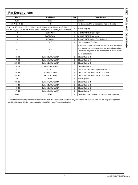
● — LMK01000: 3 LVDS outputs (CLKout0 - CLKout2) + 5 LVPECL outputs (CLKout3 - CLKout7) — LMK01010: 8 LVDS outputs — LMK01020: 8 LVPECL outputs — Channel divider values of 1, 2 to 510 (even divides) — Programmable output skew control External synchronization Pin compatible family of clocking devices 3.15 to 3.45 V operation Package: 48 pin LLP (7.0 x 7.0 x 0.8 mm) Target
APPLICATIONS
●●
●
●
●
● High performance Clock Distribution Wireless Infrastructure Medical Imaging Wired Communications Test and Measurement Military / Aerospace System Diagram 30042806 TRI-STATE® is a registered trademark of National Semiconductor Corporation. © 2008 National Semiconductor Corpo...