LMK03000C
LMK03000C is Precision Clock Conditioner manufactured by National Semiconductor.
- Part of the LMK03000 comparator family.
Description
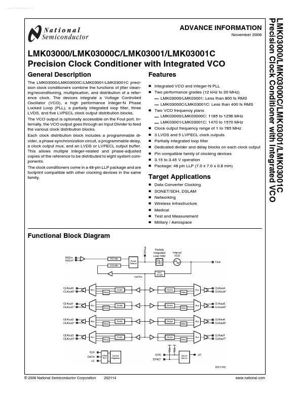
The LMK03000/LMK03000C/LMK03001/LMK03001C precision clock conditioners bine the functions of jitter cleaning/reconditioning, multiplication, and distribution of a reference clock. The devices integrate a Voltage Controlled Oscillator (VCO), a high performance Integer-N Phase Locked Loop (PLL), a partially integrated loop filter, three LVDS, and five LVPECL clock output distribution blocks. The VCO output is optionally accessible on the Fout port. Internally, the VCO output goes through an Input Divider to feed the various clock distribution blocks. Each clock distribution block includes a programmable divider, a phase synchronization circuit, a programmable delay, a clock output mux, and an LVDS or LVPECL output buffer. This allows multiple integer-related and phase-adjusted copies of the reference to be distributed to eight system ponents. The clock conditioners e in a 48-pin LLP package and are footprint patible with other clocking devices in the same family.
Features
- Integrated VCO and Integer-N PLL
- Two performance grades (12 k Hz to 20 MHz)
- -
- -
- -
- -
- LMK03000/LMK03001: Less than 800 fs RMS
- LMK03000C/LMK03001C: Less than 400 fs RMS Two VCO frequency plans
- LMK03000/LMK03000C: 1185 to 1296 MHz
- LMK03001/LMK03001C: 1470 to 1570 MHz Clock output frequency range of 1 to 785 MHz 3 LVDS and 5 LVPECL clock outputs Partially integrated loop filter Dedicated divider and delay blocks on each clock output Pin patible family of clocking devices 3.15 to 3.45 V operation Package: 48 pin LLP (7.0 x 7.0 x 0.8 mm)
Target Applications
- -
- -
- -
- Data Converter Clocking SONET/SDH, DSLAM Networking Wireless Infrastructure Medical Test and Measurement Military / Aerospace
Functional Block Diagram
© 2006 National Semiconductor Corporation
.national.
LMK03000/LMK03000C/LMK03001/LMK03001C
Connection Diagram
48-Pin LLP Package
Pin Descriptions
Pin # 1, 25 2 Pin Name GND Fout I/O O I I I I O O O O O I I O I O O O O Ground...