LMK03200
LMK03200 is Precision 0-Delay Clock Conditioner manufactured by National Semiconductor.
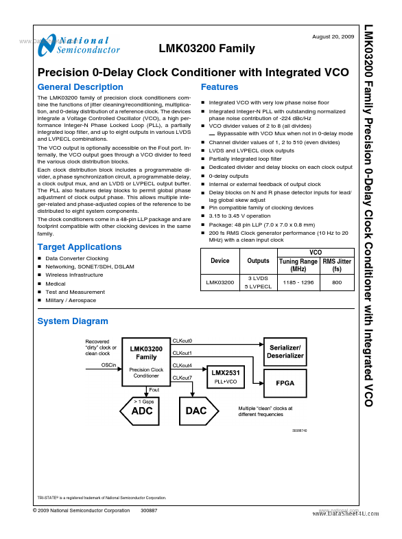
LMK03200 Family Precision 0-Delay Clock Conditioner with Integrated VCO
..
August 20, 2009
LMK03200 Family
Precision 0-Delay Clock Conditioner with Integrated VCO
General Description
The LMK03200 family of precision clock conditioners bine the functions of jitter cleaning/reconditioning, multiplication, and 0-delay distribution of a reference clock. The devices integrate a Voltage Controlled Oscillator (VCO), a high performance Integer-N Phase Locked Loop (PLL), a partially integrated loop filter, and up to eight outputs in various LVDS and LVPECL binations. The VCO output is optionally accessible on the Fout port. Internally, the VCO output goes through a VCO divider to feed the various clock distribution blocks. Each clock distribution block includes a programmable divider, a phase synchronization circuit, a programmable delay, a clock output mux, and an LVDS or LVPECL output buffer. The PLL also Features delay blocks to permit global phase adjustment of clock output phase. This allows multiple integer-related and phase-adjusted copies of the reference to be distributed to eight system ponents. The clock conditioners e in a 48-pin LLP package and are footprint patible with other clocking devices in the same family.
Features
- Integrated VCO with very low phase noise floor
- Integrated Integer-N PLL with outstanding normalized phase noise contribution of -224 d Bc/Hz
- VCO divider values of 2 to 8 (all divides)
- -
- -
- -
- -
- -
- - Bypassable with VCO Mux when not in 0-delay mode Channel divider values of 1, 2 to 510 (even divides) LVDS and LVPECL clock outputs Partially integrated loop filter Dedicated divider and delay blocks on each clock output 0-delay outputs Internal or external feedback of output clock Delay blocks on N and R phase detector inputs for lead/ lag global skew adjust Pin patible family of clocking devices 3.15 to 3.45 V operation Package: 48 pin LLP (7.0 x 7.0 x 0.8 mm) 200 fs RMS Clock generator...