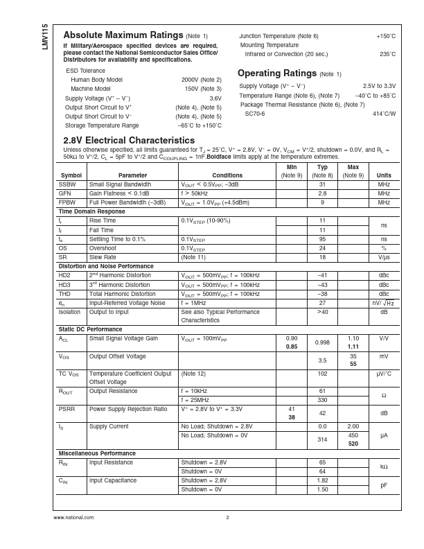
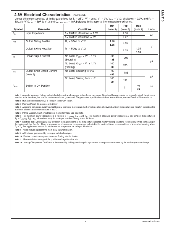
LMV115 Overview
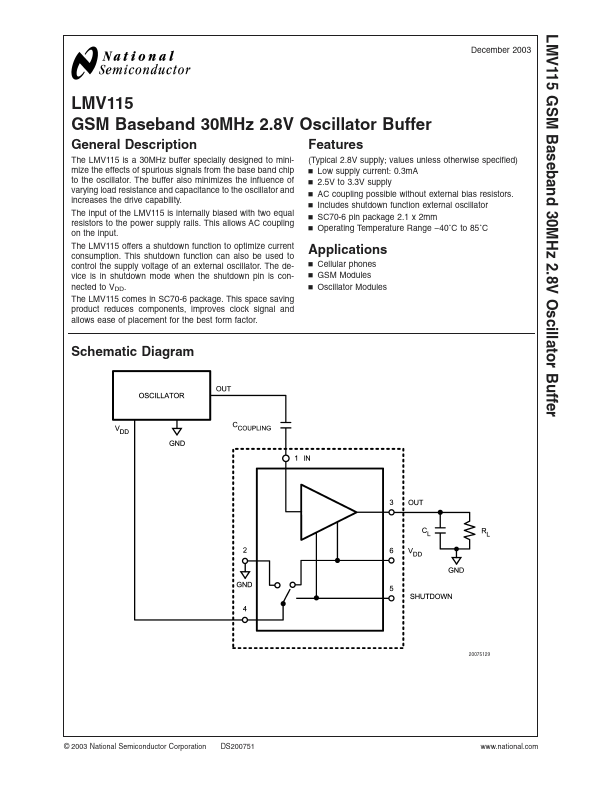
The LMV115 is a 30MHz buffer specially designed to minimize the effects of spurious signals from the base band chip to the oscillator. The buffer also minimizes the influence of varying load resistance and capacitance to the oscillator and increases the drive capability. The input of the LMV115 is internally biased with two equal resistors to the power supply rails.