MH0012C
Overview
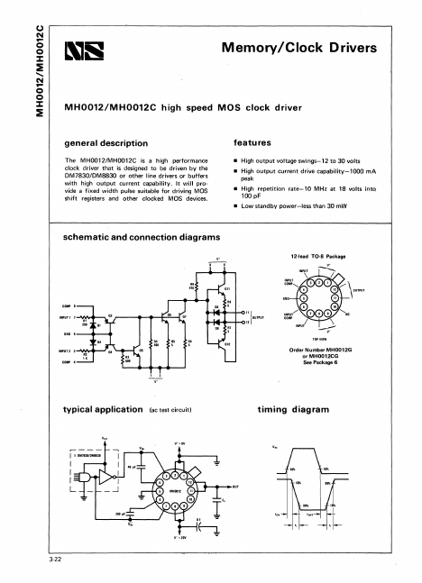
The MH0012/MH0012C is a high performance clock driver that is designed to be driven by the DM7830/DM8830 or other line drivers or buffers with high output current capability. It will provide a fixed width pulse suitable for driving MOS shift registers and other clocked MOS devices.
- High output voltage swings-12 to 30 volts
- High output current drive capability-lOOO mA peak
- High repetition rate-lO MHz at 18 volts into 100 pF
- Low standby power-less than 30 mW schematic and connection diagrams y'
- 9 COMP 8