National Semiconductor MM74C157
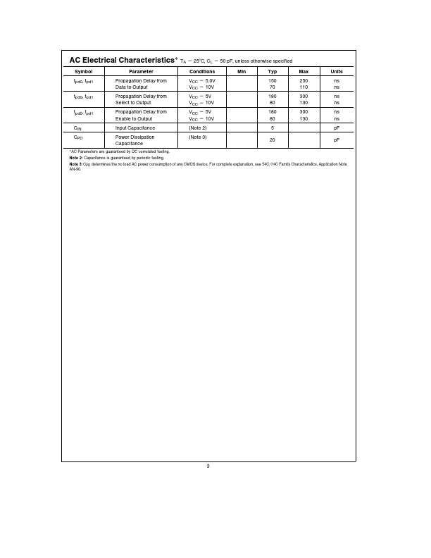
The table of ‘‘Electrical Characteristics’’ provides conditions for actual device operation 2 AC Electrical Characteristics Symbol tpd0 tpd1 tpd0 tpd1 tpd0 tpd1 CIN CPD Parameter Propagation Delay from Data to Output Propagation Delay from Select to Output Propagation Delay from Enable to Output Input Capacitance Power Dissipation Capacitance TA e 25 C CL e 50 pF unless otherwise specified Conditions VCC e 5 0V VCC e 10V VCC e 5V VCC e 10V VCC e 5V VCC e 10V (Note 2) (Note 3) Min Typ 150 70 180 80 180 80 5 20 Max 250 110 300 130 300 130 Units ns ns ns ns ns ns pF pF AC Parameters are...| Part No. | MM74C157 |
|---|---|
| Datasheet | MM74C157 Download |
| Manufacturer |  National Semiconductor |
| Description | Quad 2-Input Multiplexers |
| Buy | Stock & Price |

GENERAL DESCRIPTION
These multiplexers are monolithic complementary MOS (CMOS) integrated circuits constructed with N- and P-channel enhancement transistors They consist of four 2-input multiplexers with common select and enable inputs When the enable input is at logical ‘‘0’’ the four outputs assume the values as selected from the inputs When the enable input is at logical ‘‘1’’ the outputs assume logical ‘‘0’’ Select decoding is done internally resulting in a single select input onlyFEATURES
Y Y Y Y Supply voltage range High noise immunity Low power Tenth power TTL compatible 3V to 15V 0 45 VCC (typ ) 50 nW (typ ) Drive 2 LPTTL loads Logic Connection Diagrams Dual-In-Line Package TL F 5894 – 2 Top View Order Number MM54C157 or MM74C157 TL F 5894 – 1 Truth Table Enable 1 0 0 0 0 Select X 0 0 1 1 A X 0 1 X X B X X X 0 1 Output Y 0 0 1 0 1 Guaranteed Noise Margin as a Function of VCC 74L Compatibility TL F 5894 – 4 TL F 5894 – 3 C1995 National Semiconductor Corporation TL F 5894 RRD-B3...