National Semiconductor OP-07
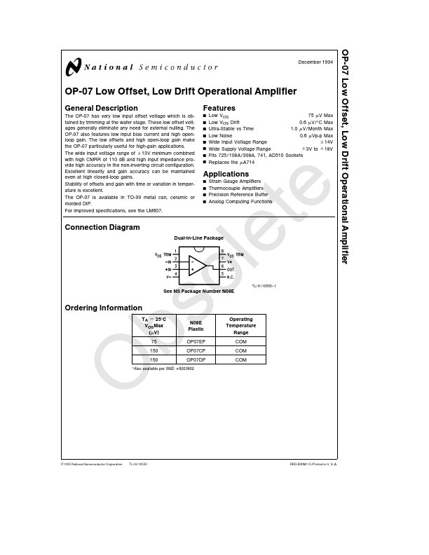
The OP-07 has very low input offset voltage which is ob- Y Low VOS 75 mV Max tained by trimming at the wafer stage These low offset volt- Y Low VOS Drift 0 6 mV C Max ages generally eliminate any need for external nulling The Y Ultra-Stable vs Time 1 0 mV Month Max OP-07 also features low input bias current and high open- Y Low Noise 0 6 mVp-p Max loop gain The low offsets and high open-loop gain make Y Wide Input Voltage Range g14V the OP-07 particularly useful for high-gain applications Y Wide Supply Voltage Range g3V to g18V The wide input voltage range of g13V minimum combined Y Fits 725...| Part No. | OP-07 |
|---|---|
| Datasheet | OP-07 Download |
| Manufacturer |  National Semiconductor |
| Description | Low Drift Operational Amplifier |
| Buy | Stock & Price |