GENERAL DESCRIPTION
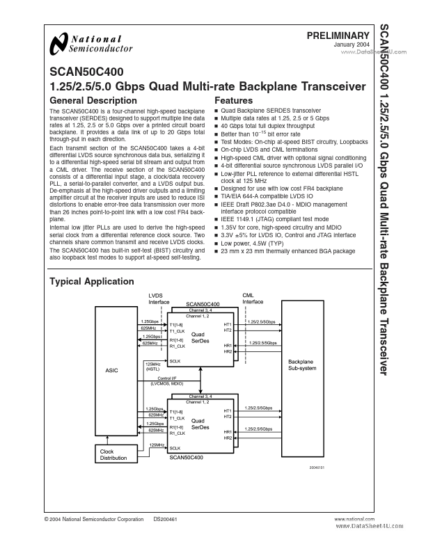
The receive section of the SCAN50C400 consists of a differential input stage, a clock/data recovery PLL, a serial-to-parallel converter, and a LVDS output bus. De-emphasis at the high-speed driver outputs and a limiting amplifier circuit at the receiver inputs are used to reduce ISI distortions to enable error-free data transmission over more than 26 inches point-to-point link with a low cost FR4 backplane. Internal low jitter PLLs are used to derive the high-speed serial clock from a differential reference clock source. Two channels share common transmit and receive LVDS clocks. The SCAN50C400 has built-in self-test (BIST) circuitry and also loopback test modes to support at-speed self-testing. FEATURES
n n n n n n n n n n n n n n n n n Quad Backplane SERDES transceiver Multiple data rates at 1.25, 2.5 or 5 Gbps 40 Gbps total full duplex throughput Better than 10−15 bit error rate Test Modes: On-chip at-speed BIST circuitry, Loopbacks On-chip LVDS and CML terminati... National Semiconductor