74F410
74F410 is Register Stack16 x 4 RAM TRI-STATEE Output Register manufactured by National Semiconductor.
Description
The ’F410 is a register-oriented high-speed 64-bit Read Write Memory organized as 16-words by 4-bits An edgetriggered 4-bit output register allows new input data to be written while previous data is held TRI-STATE outputs are provided for maximum versatility The ’F410 is fully patible with all TTL families
Features
Y Y Y Y Y Y
Edge-triggered output register Typical access time of 35 ns TRI-STATE outputs Optimized for register stack operation 18-pin package 9410 replacement
16 x 4 RAM TRI-STATE Output Register mercial 74F410PC
Military
Package Number N18A
Package Description
18-Lead (0 300 Wide) Molded Dual-In-Line 18-Lead Ceramic Dual-In-Line 20-Lead (0 300 Wide) Molded Small Outline JEDEC 20-Lead Cerpak
54F410DM (Note 1) 74F410SC 54F410LM
J18A M20B W20A
Note 1 Military grade device with environmental and burn-in processing Use suffix e DMQB LMQB
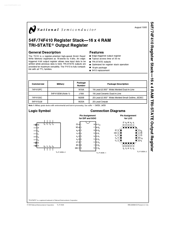
Logic Symbol
Connection Diagrams
Pin Assignment for DIP and SOIC Pin Assignment for LCC
TL F 9538- 3
TL F 9538
- 1
TL F 9538
- 2
TRI-STATE is a registered trademark of National Semiconductor Corporation C1995 National Semiconductor Corporation TL F 9538 RRD-B30M105 Printed in U S A
Unit Loading Fan Out
54F 74F Pin Names Description
UL HIGH LOW 10 10 10 10 10 10 10 20 10 10 Input IIH IIL Output IOH IOL 20 m A 20 m A 20 m A 20 m A 20 m A b 0 6 m A b 0 6 m A b 1 2 m A b 0 6 m A b 0 6 m A
A0
- A3 D 0
- D3 CS OE WE CP Q0
- Q3
Address Inputs Data Inputs Chip Select Input (Active LOW) Output Enable Input (Active LOW) Write Enable Input (Active LOW) Clock Input (Outputs Change on LOW-to-HIGH Transition) TRI-STATE Outputs
10 20 150 40 (33 3)
20 m A b1 2 m A b 3 m A 24 m A (20 m A)
Functional Description
Write Operation When the three control inputs Write Enable (WE) Chip Select (CS) and Clock (CP) are LOW the information on the data inputs (D0
- D3) is written into the memory location selected by the address inputs (A0
- A3) If the input data changes while WE CS and CP are LOW the contents of the selected memory...