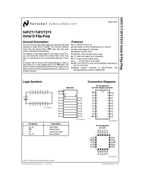
74FCT273 Description
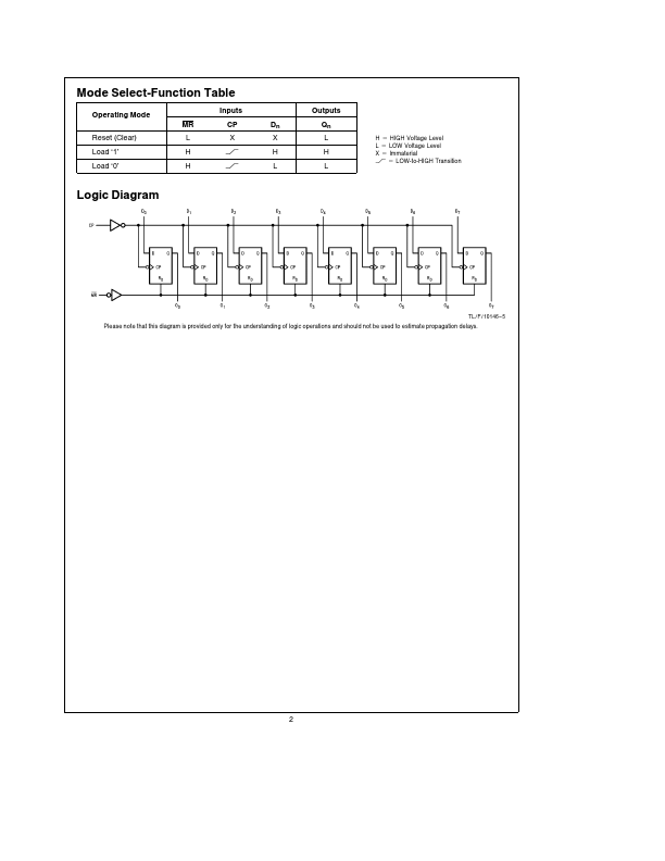
The ’FCT273 has eight edge-triggered D-type flip-flops with individual D inputs and Q outputs The mon buffered Clock (CP) and Master Reset (MR) input load and reset (clear) all flip-flops simultaneously The register is fully edge-triggered The state of each D input one setup time before the LOW-to-HIGH clock transition is transferred to the corresponding flip-flop’s Q output All outputs will be forced LOW...
74FCT273 Key Features
- 2 TL F 10146