DM74LS962
Description
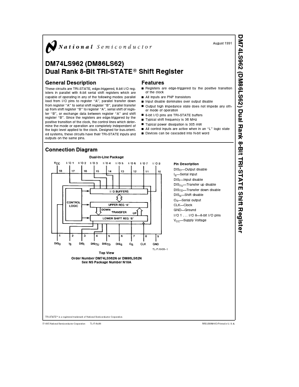
These circuits are TRI-STATE edge-triggered 8-bit I O registers in parallel with 8-bit serial shift registers which are capable of operating in any of the following modes parallel load from I O pins to register ‘‘A’’ parallel transfer down from register ‘‘A’’ to serial shift register ‘‘B’’ parallel transfer up from shift register ‘‘B’’ to register ‘‘A’’ serial shift of register ‘‘B’’ or exchange data between register ‘‘A’’ and shift register ‘‘B’’ Since the registers are edge-triggered by the positive transition of the clock the control lines which determine the mode or operation are pletely independent of the logic level applied to the clock Designed for bus-oriented systems these circuits have their TRI-STATE inputs and outputs on the same pins
Features
Y Y Y Y Y
Registers are edge-triggered by the positive transition of the clock All inputs are PNP transistors Input disable dominates over output disable Output high impedance state does not impede any other...