54F74
54F74 is Dual D-Type Positive Edge-Triggered Flip-Flop manufactured by National Semiconductor.
Description
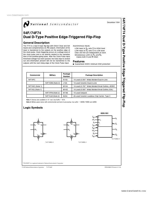
The ’F74 is a dual D-type flip-flop with Direct Clear and Set inputs and plementary (Q Q) outputs Information at the input is transferred to the outputs on the positive edge of the clock pulse Clock triggering occurs at a voltage level of the clock pulse and is not directly related to the transition time of the positive-going pulse After the Clock Pulse input threshold voltage has been passed the Data input is locked out and information present will not be transferred to the outputs until the next rising edge of the Clock Pulse input Asynchronous Inputs LOW input to SD sets Q to HIGH level LOW input to CD sets Q to LOW level Clear and Set are independent of clock Simultaneous LOW on CD and SD makes both Q and Q HIGH
Features
Guaranteed 4000V minimum ESD protection mercial 74F74PC
Military
Package Number N14A
Package Description
14-Lead (0 300 Wide) Molded Dual-In-Line 14-Lead Ceramic Dual-In-Line 14-Lead (0 150 Wide) Molded Small Outline JEDEC 14-Lead (0 300 Wide) Molded Small Outline EIAJ 14-Lead Cerpack 20-Lead Ceramic Leadless Chip Carrier Type C
54F74DM (Note 2) 74F74SC (Note 1) 74F74SJ (Note 1) 54F74FM (Note 2) 54F74LM (Note 2)
J14A M14A M14D W14B E20A
Note 1 Devices also available in 13 reel Use Suffix e SCX Note 2 Military grade device with environmental and burn-in processing Use suffix e DMQB FMQB and LMQB
Logic Symbols
IEEE IEC
TL F 9469
- 6 TL F 9469- 3 TL F 9469
- 4
TRI-STATE is a registered trademark of National Semiconductor Corporation C1995 National Semiconductor Corporation
TL F 9469
RRD-B30M75 Printed in U S A
..
Connection Diagrams
Pin Assignment for DIP SOIC and Flatpak Pin Assignment for LCC
TL F 9469- 1
TL F 9469
- 2
Unit Loading Fan Out
54F 74F Pin Names Description
UL HIGH LOW 10 10 10 10 10 30 10 30 50 33 3 Input IIH IIL Output IOH IOL 20 m A b0 6 m A 20 m A b0 6 m A 20 m A b1 8 m A 20 m A b1 8 m A b 1 m A 20 m A
D1 D2 CP1 CP2 CD1 CD2 SD1 SD2 Q1 Q1 Q2 Q2
Data Inputs Clock Pulse Inputs (Active Rising Edge) Direct Clear...