CD4014BM
CD4014BM is 8-Stage Static Shift Register manufactured by National Semiconductor.
Description
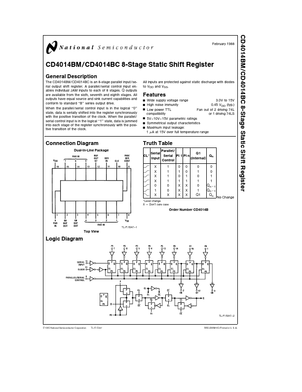
The CD4014BM CD4014BC is an 8-stage parallel input serial output shift register A parallel serial control input enables individual JAM inputs to each of 8 stages Q outputs are available from the sixth seventh and eighth stages All outputs have equal source and sink current capabilities and conform to standard ‘‘B’’ series output drive When the parallel serial control input is in the logical ‘‘0’’ state data is serially shifted into the register synchronously with the positive transition of the clock When the parallel serial control input is in the logical ‘‘1’’ state data is jammed into each stage of the register synchronously with the positive transition of the clock All inputs are protected against static discharge with diodes to VDD and VSS
Features
Wide supply voltage range 3 0V to 15V High noise immunity 0 45 VDD (typ ) Low power TTL Fan out of 2 driving 74L patibility or 1 driving 74LS 5V
- 10V
- 15V parametric ratings Symmetrical output characteristics Maximum input leakage 1 m A at 15V over full temperature range
Connection Diagram
Dual-In-Line Package
Truth Table
CL L L L L L L K Parallel Serial Q1 Serial PI 1 PI n Qn Input (Internal) Control X X X X 0 1 X 1 1 1 1 0 0 X 0 1 0 1 X X X 0 0 1 1 X X X 0 1 0 1 0 1 Q1 0 0 1 1 Qnb1 Qnb1 Qn
No Change
Level change X e Don’t care case
Order Number CD4014B
TL F 5947
- 1
Top View
Logic Diagram
TL F 5947
- 2
C1995 National Semiconductor Corporation
TL F 5947
RRD-B30M105 Printed in U S A
Absolute Maximum Ratings (Notes 1
2)
If Military Aerospace specified devices are required please contact the National Semiconductor Sales Office Distributors for availability and specifications Supply Voltage (VDD) Input Voltage (VIN) Storage Temperature Range (TS) Power Dissipation (PD) Dual-In-Line Small Outline Lead Temperature (TL) (Soldering 10 seconds) b 0 5V to a 18V b 0 5 to VDD a 0 5V b 65 C to a 150 C
Remended Operating Conditions (Note 2)
Supply Voltage (VDD) Input Voltage (VIN)...