CD4015BM
CD4015BM is Dual 4-Bit Static Shift Register manufactured by National Semiconductor.
Description
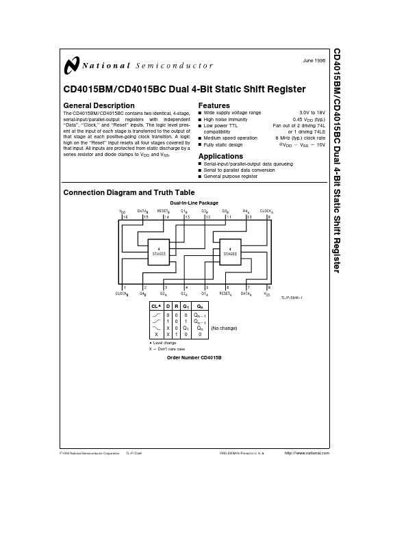
The CD4015BM CD4015BC contains two identical 4-stage serial-input parallel-output registers with independent ‘‘Data’’ ‘‘Clock ’’ and ‘‘Reset’’ inputs The logic level present at the input of each stage is transferred to the output of that stage at each positive-going clock transition A logic high on the ‘‘Reset’’ input resets all four stages covered by that input All inputs are protected from static discharge by a series resistor and diode clamps to VDD and VSS
Features
Wide supply voltage range High noise immunity Low power TTL patibility Medium speed operation Fully static design
3 0V to 18V 0 45 VDD (typ ) Fan out of 2 driving 74L or 1 driving 74LS 8 MHz (typ ) clock rate VDD b VSS e 10V
Applications
Serial-input parallel-output data queueing Serial to parallel data conversion General purpose register
Connection Diagram and Truth Table
Dual-In-Line Package
TL F 5948
- 1
CL U L L K X
D 0 1 X X
R 0 0 0 1
Q1 0 1 Q1 0
Qn Qnb1 Qnb1 Qn 0
(No change)
U Level change
X e Don’t care case
Order Number CD4015B
C1996 National Semiconductor Corporation
TL F 5948
RRD-B30M76 Printed in U S A http
national
Absolute Maximum Ratings (Notes 1
2)
If Military Aerospace specified devices are required please contact the National Semiconductor Sales Office Distributors for availability and specifications DC Supply Voltage (VDD) Input Voltage (VIN) Storage Temperature Range (TS) Power Dissipation (PD) Dual-In-Line Small Outline Lead Temperature (TL) (Soldering 10 seconds) b 0 5 to a 18 VDC b 0 5 to VDD a 0 5 VDC b 65 C to a 150 C
Remended Operating Conditions
DC Supply Voltage (VDD) Input Voltage (VIN) Operating Temperature Range (TA) CD4015BM CD4015BC a 3 to a 15 VDC
0 to VDD VDC b 55 C to a 125 C b 40 C to a 85 C
700 m W 500 m W 260 C
DC Electrical Characteristics CD4015BM (Note 2)
Symbol IDD Parameter Quiescent Device Current Low Level Output Voltage High Level Output Voltage Low Level Input Voltage High Level Input Voltage Low...