CD4016BC
CD4016BC is Quad Bilateral Switch manufactured by National Semiconductor.
Description
The CD4016BM CD4016BC is a quad bilateral switch intended for the transmission or multiplexing of analog or digital signals It is pin-for-pin patible with CD4066BM CD4066BC
Extremely high control input impedance 1012X (typ ) b 50 d B (typ ) Low crosstalk between switches f IS e 0 9 MHz RL e 1 k X Frequency response switch ‘‘ON’’ 40 MHz (typ )
Features
Wide supply voltage range 3V to 15V Wide range of digital and analog switching g 7 5 VPEAK ‘‘ON’’ resistance for 15V operation 400X (typ ) Matched ‘‘ON’’ resistance over 15V signal input DRON e 10X (typ ) High degree of linearity 0 4% distortion (typ ) f IS e 1 k Hz VIS e 5 Vp-p VDDb VSS e 10V RL e 10 k X Extremely low ‘‘OFF’’ switch leakage 0 1 n A (typ ) VDD b VSS e 10V TA e 25 C
Applications
Analog signal switching multiplexing Signal gating Squelch control Chopper Modulator Demodulator mutating switch Digital signal switching multiplexing CMOS logic implementation Analog-to-digital digital-to-analog conversion Digital control of frequency impedance phase and analog-signal gain
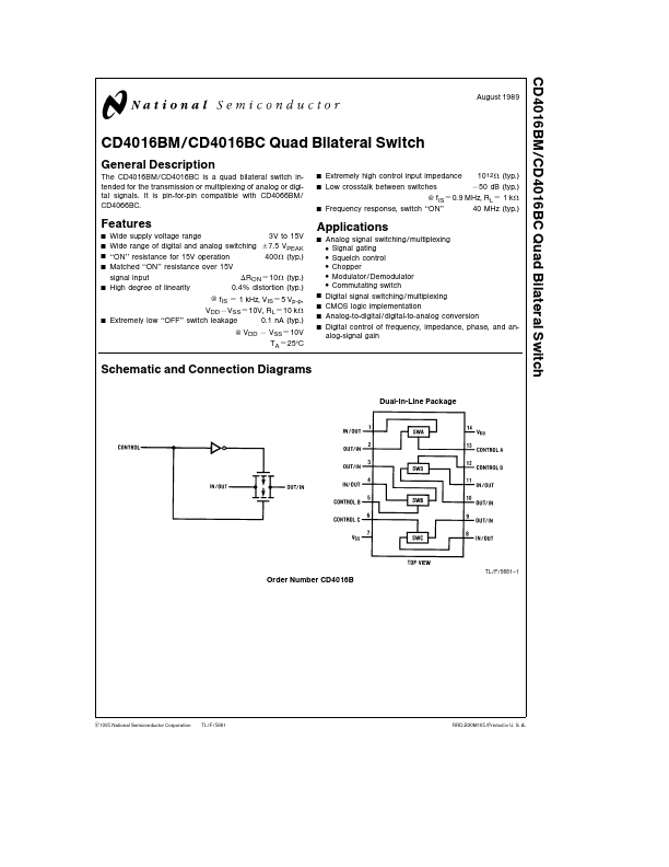
Schematic and Connection Diagrams
Dual-In-Line Package
TL F 5661
- 1
Order Number CD4016B
C1995 National Semiconductor Corporation
TL F 5661
RRD-B30M105 Printed in U S A
Absolute Maximum Ratings
If Military Aerospace specified devices are required please contact the National Semiconductor Sales Office Distributors for availability and specifications b 0 5V to a 18V b 0 5V to VDD a 0 5V VIN Input Voltage b 65 C to a 150 C TS Storage Temperature Range Power Dissipation (PD) Dual-In-Line 700 m W Small Outline 500 m W Lead Temperature (Soldering 10 seconds) 260 C
Remended Operating Conditions (Note 2)
VDD Supply Voltage VIN Input Voltage TA Operating Temperature Range CD4016BM CD4016BC 3V to 15V 0V to VDD b 55 C to a 125 C b 40 C to a 85 C
(Notes 1 and 2) VDD Supply Voltage
DC Electrical Characteristics CD4016BM (Note 2)
Symbol IDD Parameter Quiescent Device Current Conditions VDD e 5V...