CD4019BC
CD4019BC is Quad AND-OR Select Gate manufactured by National Semiconductor.
Description
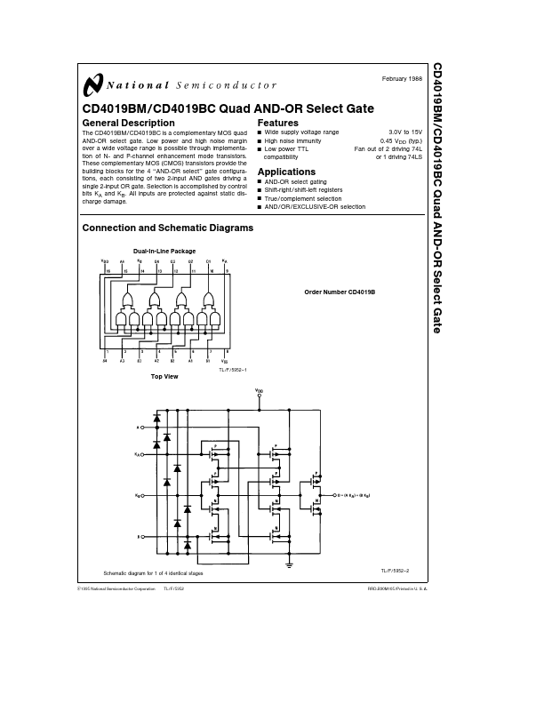
The CD4019BM CD4019BC is a plementary MOS quad AND-OR select gate Low power and high noise margin over a wide voltage range is possible through implementation of N- and P-channel enhancement mode transistors These plementary MOS (CMOS) transistors provide the building blocks for the 4 ‘‘AND-OR select’’ gate configurations each consisting of two 2-input AND gates driving a single 2-input OR gate Selection is acplished by control bits KA and KB All inputs are protected against static discharge damage
Features
Wide supply voltage range High noise immunity Low power TTL patibility
3 0V to 15V 0 45 VDD (typ ) Fan out of 2 driving 74L or 1 driving 74LS
Applications
AND-OR select gating Shift-right shift-left registers True plement selection AND OR EXCLUSIVE-OR selection
Connection and Schematic Diagrams
Dual-In-Line Package
Order Number CD4019B
TL F 5952
- 1
Top View
Schematic diagram for 1 of 4 identical stages
C1995 National Semiconductor Corporation TL F 5952
TL F 5952
- 2
RRD-B30M105 Printed in U S A
Absolute Maximum Ratings (Notes 1
2)
If Military Aerospace specified devices are required please contact the National Semiconductor Sales Office Distributors for availability and specifications Supply Voltage (VDD) Input Voltage (VIN) Storage Temperature Range (TS) Power Dissipation (PD) Dual-In-Line Small Outline Lead Temperature (TL) (Soldering 10 seconds) b 0 5V to a 18V b 0 5V to VDD a 0 5V b 65 C to a 150 C
Remended Operation Conditions (Note 2)
DC Supply Voltage (VDD) Input Voltage (VIN) Operating Temperature Range (TA) CD4019BM CD4019BC a 3V to a 15V
0V to VDD V b 55 C to a 125 C b 40 C to a 85 C
700 m W 500 m W 260 C
DC Electrical Characteristics CD4019BM (Note 2)
Symbol IDD Parameter Quiescent Device Current Low Level Output Voltage Conditions VDD e 5V VDD e 10V VDD e 15V b 55 C a 25 C a 125 C
Units m A m A m A V V V V V V
Min
Max 0 25 05 10 0 05 0 05 0 05
Min
Typ 0 03 0 05 0 07 0 0 0
Max 0 25 05 10 0 05 0 05 0...