CD4041UBC
CD4041UBC is Quad True/Complement Buffer manufactured by National Semiconductor.
Description
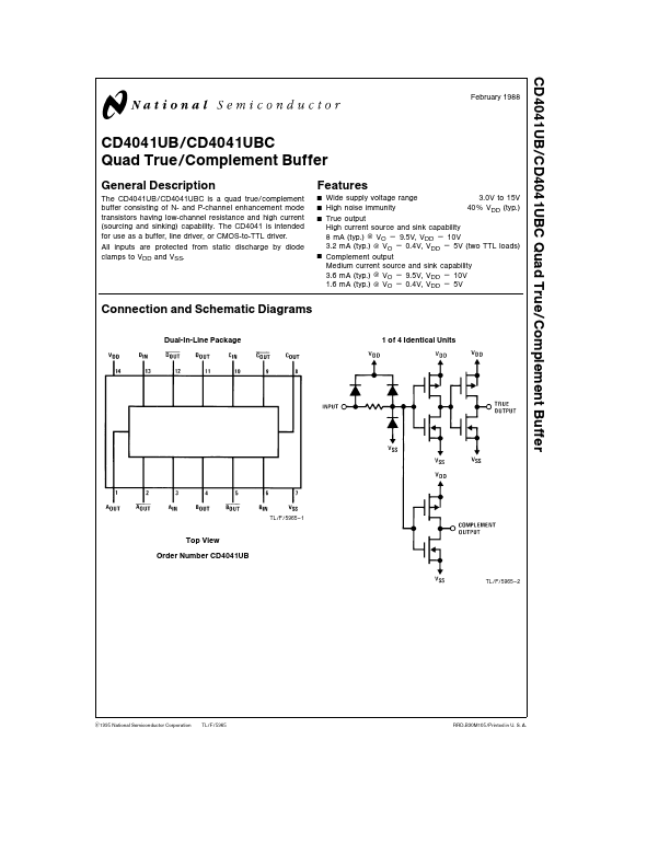
The CD4041UB CD4041UBC is a quad true plement buffer consisting of N- and P-channel enhancement mode transistors having low-channel resistance and high current (sourcing and sinking) capability The CD4041 is intended for use as a buffer line driver or CMOS-to-TTL driver All inputs are protected from static discharge by diode clamps to VDD and VSS
Features
Wide supply voltage range 3 0V to 15V High noise immunity 40% VDD (typ ) True output High current source and sink capability 8 m A (typ ) VO e 9 5V VDD e 10V 3 2 m A (typ ) VO e 0 4V VDD e 5V (two TTL loads) plement output Medium current source and sink capability 3 6 m A (typ ) VO e 9 5V VDD e 10V 1 6 m A (typ ) VO e 0 4V VDD e 5V
Connection and Schematic Diagrams
Dual-In-Line Package 1 of 4 Identical Units
TL F 5965
- 1
Top View Order Number CD4041UB
TL F 5965
- 2
C1995 National Semiconductor Corporation
TL F 5965
RRD-B30M105 Printed in U S A
Absolute Maximum Ratings
(Notes 1 and 2)
If Military Aerospace specified devices are required please contact the National Semiconductor Sales Office Distributors for availability and specifications b 0 5V to a 18V Supply Voltage (VDD) b 0 5V to VDD a 0 5V Input Voltage (VIN) b 65 C to a 150 C Storage Temperature Range (TS) Power Dissipation (PD) Dual-In-Line 700 m W Small Outline 500 m W Lead Temp (TL) (Soldering 10 sec ) 260 C
Remended Operating Conditions (Note 2)
Supply Voltage (VDD) Input Voltage (VIN) Operating Temperature Range (TA) CD4041UB CD4041UBC 3V to 15V 0V to VDD b 55 C to a 125 C b 40 C to a 85 C
DC Electrical Characteristics CD4041UBM (Note 2)
Symbol IDD Parameter Conditions b 55 C a 25 C a 125 C
Units m A m A m A V V V V V V
Min Quiescent Device Current VDD e 5V VDD e 10V VDD e 15V Low Level Output Voltage
Max 1 2 4 0 05 0 05 0 05
Min
Typ 0 01 0 01 0 01 0 0 0
Max 1 2 4 0 05 0 05 0 05
Min
Max 30 60 120 0 05 0 05 0 05
VOL l IOl k 1 m A VIL e 0V VIH e VDD VDD e 5V VDD e 10V VDD e 15V
High Level Output Voltage l IOl k 1 m A...