CD4066BM
CD4066BM is Quad Bilateral Switch manufactured by National Semiconductor.
Description
The CD4066BM CD4066BC is a quad bilateral switch intended for the transmission or multiplexing of analog or digital signals It is pin-for-pin patible with CD4016BM CD4016BC but has a much lower ‘‘ON’’ resistance and ‘‘ON’’ resistance is relatively constant over the input-signal range
Extremely low ‘‘OFF’’ 0 1 n A (typ ) switch leakage VDDb VSS e 10V TA e 25 C Extremely high control input impedance 1012X(typ ) b 50 d B (typ ) Low crosstalk between switches fis e 0 9 MHz RL e 1 k X Frequency response switch ‘‘ON’’ 40 MHz (typ )
Features
Wide supply voltage range 3V to 15V High noise immunity 0 45 VDD (typ ) g 7 5 VPEAK Wide range of digital and analog switching ‘‘ON’’ resistance for 15V operation 80X Matched ‘‘ON’’ resistance DRON e 5X (typ ) over 15V signal input ‘‘ON’’ resistance flat over peak-to-peak signal range High ‘‘ON’’ ‘‘OFF’’ 65 d B (typ ) output voltage ratio fis e 10 k Hz RL e 10 k X High degree linearity 0 1% distortion (typ ) High degree linearity fis e 1 k Hz Vis e 5Vp-p High degree linearity VDDb VSS e 10V RL e 10 k X
Applications
Analog signal switching multiplexing Signal gating Squelch control Chopper Modulator Demodulator mutating switch Digital signal switching multiplexing CMOS logic implementation Analog-to-digital digital-to-analog conversion Digital control of frequency impedance phase and analog-signal-gain
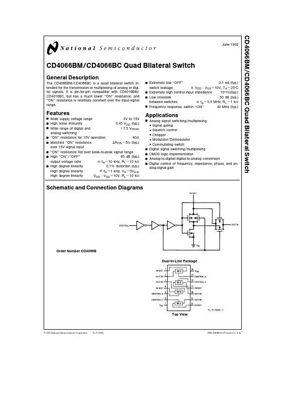
Schematic and Connection Diagrams
Order Number CD4066B Dual-In-Line Package
TL F 5665
- 1
Top View
C1995 National Semiconductor Corporation
TL F 5665
RRD-B30M105 Printed in U S A
Absolute Maximum Ratings (Notes 1
2)
If Military Aerospace specified devices are required please contact the National Semiconductor Sales Office Distributors for availability and specifications Supply Voltage (VDD) Input Voltage (VIN) Storage Temperature Range (TS) Power Dissipation (PD) Dual-In-Line Small Outline Lead Temperature (TL) (Soldering 10 seconds) b 0 5V to a 18V b 0 5V to VDD a 0 5V b...