CD4515BM
CD4515BM is 4-Bit Latched/4-to-16 Line Decoders manufactured by National Semiconductor.
Description
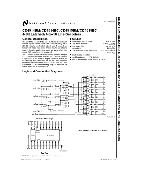
The CD4514B and CD4515B are 4-to-16 line decoders with latched inputs implemented with plementary MOS (CMOS) circuits constructed with N- and P-channel enhancement mode transistors These circuits are primarily used in decoding applications where low power dissipation and or high noise immunity is required The CD4514B (output active high option) presents a logical ‘‘1’’ at the selected output whereas the CD4515B presents a logical ‘‘0’’ at the selected output The input latches are R
- S type flip-flops which hold the last input data presented prior to the strobe transition from ‘‘1’’ to ‘‘0’’ This input data is decoded and the corresponding output is activated An output inhibit line is also available
Features
Wide supply voltage range High noise immunity Low power TTL patibility Low quiescent power dissipation
3 0V to 15V 0 45 VDD (typ ) fan out of 2 driving 74L 0 025 m W package 5 0 VDC
Single supply operation Input impedance e 1012X typically Plug-in replacement for MC14514 MC14515
Logic and Connection Diagrams
TL F 5994
- 1
Dual-In-Line Package
Order Number CD4514B or CD4515B
TL F 5994
- 2
Top View
TRI-STATE is a registered trademark of National Semiconductor Corporation C1995 National Semiconductor Corporation
TL F 5994
RRD-B30M105 Printed in U S A
Absolute Maximum Ratings (Notes 1 and 2)
If Military Aerospace specified devices are required please contact the National Semiconductor Sales Office Distributors for availability and specifications DC Supply Voltage (VDD) Input Voltage (VIN) Storage Temperature Range (TS) Power Dissipation (PD) Dual-In-Line Small Outline Lead Temperature (TL) (Soldering 10 seconds) b 0 5V to a 18V b 0 5V to VDD a 0 5V b 65 C to a 150 C
Remended Operating Conditions (Note 2)
DC Supply Voltage (VDD) Input Voltage (VIN) Operating Temperature Range (TA) CD4514BM CD4515BM CD4514BC CD4515BC 3V to 15V 0V to VDD b 55 C to a 125 C b 40 C to a 85 C
700 m W 500 m W 260 C CD4515BM (Note 2) b 55 C a 25 C a...