D4001BC
D4001BC is CD4001BC manufactured by National Semiconductor.
Description
These quad gates are monolithic plementary MOS (CMOS) integrated circuits constructed with N- and P-channel enhancement mode transistors They have equal source and sink current capabilities and conform to standard B series output drive The devices also have buffered outputs which improve transfer characteristics by providing very high gain All inputs are protected against static discharge with diodes to VDD and VSS
Features
Low power TTL Fan out of 2 driving 74L patibility or 1 driving 74LS 5V
- 10V
- 15V parametric ratings Symmetrical output characteristics Maximum input leakage 1 m A at 15V over full temperature range
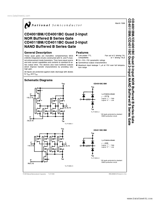
Schematic Diagrams
CD4001BC BM of device shown Je Aa B Logical ‘‘1’’ e High Logical ‘‘0’’ e Low
TL F 5939
- 2
All inputs protected by standard CMOS protection circuit
TL F 5939
- 1
CD4011BC BM of device shown Je AB Logical ‘‘1’’ e High Logical ‘‘0’’ e Low
TL F 5939
- 6
All inputs protected by standard CMOS protection circuit
TL F 5939
- 5
C1995 National Semiconductor Corporation
TL F 5939
RRD-B30M105 Printed in U S A
..
Absolute Maximum Ratings (Notes 1 and 2)
If Military Aerospace specified devices are required please contact the National Semiconductor Sales Office Distributors for availability and specifications Voltage at any Pin Power Dissipation (PD) Dual-In-Line Small Outline VDD Range Storage Temperature (TS) Lead Temperature (TL) (Soldering 10 seconds) b 0 5V to VDD a 0 5V
Operating Conditions
Operating Range (VDD) Operating Temperature Range CD4001BM CD4011BM CD4001BC CD4011BC 3 VDC to 15 VDC b 55 C to a 125 C b 40 C to a 85 C
700 m W 500 m W b 0 5 VDC to a 18 VDC b 65 C to a 150 C
260 C CD4011BM (Note 2) b 55 C a 25 C a 125 C
DC Electrical Characteristics CD4001BM
Symbol IDD Parameter Quiescent Device Current Low Level Output Voltage High Level Output Voltage Low Level Input Voltage High Level Input Voltage Low Level Output Current (Note 3) High Level Output Current (Note 3) Input Current Conditions VDD e...