DS14C239
DS14C239 is Dual Supply TIA/EIA-232 3 x 5 Driver/Receiver manufactured by National Semiconductor.
Description
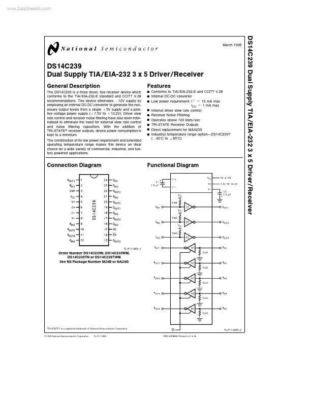
The DS14C239 is a three driver five receiver device which conforms to the TIA EIA-232-E standard and CCITT V 28 remendations This device eliminates b12V supply by employing an internal DC-DC converter to generate the necessary output levels from a single a 5V supply and a positive voltage power supply ( a 7 5V to a 13 2V) Driver slew rate control and receiver noise filtering have also been internalized to eliminate the need for external slew rate control and noise filtering capacitors With the addition of TRI-STATE receiver outputs device power consumption is kept to a minimum The bination of its low power requirement and extended operating temperature range makes this device an ideal choice for a wide variety of mercial industrial and battery powered applications
Features
Y Y Y Y Y Y
Conforms to TIA EIA-232-E and CCITT V 28 Internal DC-DC converter Low power requirement I a e 10 m A max ICC e 1 m A max Internal driver slew rate control Receiver Noise Filtering Operates above 120 kbits sec TRI-STATE Receiver Outputs Direct replacement for MAX239 Industrial temperature range option DS14C239T (b40 C to a 85 C)
Connection Diagram
Functional Diagram
TL F 11283
- 1
Order Number DS14C239N DS14C239WM DS14C239TN or DS14C239TWM See NS Package Number M24B or NA24G
TRI-STATE is a registered trademark of National Semiconductor Corporation C1996 National Semiconductor Corporation TL F 11283 RRD-B30M66 Printed in U S A
TL F 11283
- 2
Absolute Maximum Ratings (Note 1)
If Military Aerospace specified devices are required please contact the National Semiconductor Sales Office Distributors for availability and specifications b 0 3V to a 6V Supply Voltage (VCC) V a Pin (VCC b 0 3V) to a 15V a 0 3V to b 15V Vb Pin b 0 3V to (VCC a 0 3V) Driver Input Voltage Driver Output Voltage (V a a 0 3V) to (Vb b 0 3V) g 30V Receiver Input Voltage b 0 3V to (VCC a 0 3V) Receiver Output Voltage a 150 C Junction Temperature a 25 C (Note 6) Maximum Package Power Dissipation...