DS42MB200
DS42MB200 is Dual 4.25 Gbps 2:1/1:2 CML Mux/Buffer manufactured by National Semiconductor.
Description
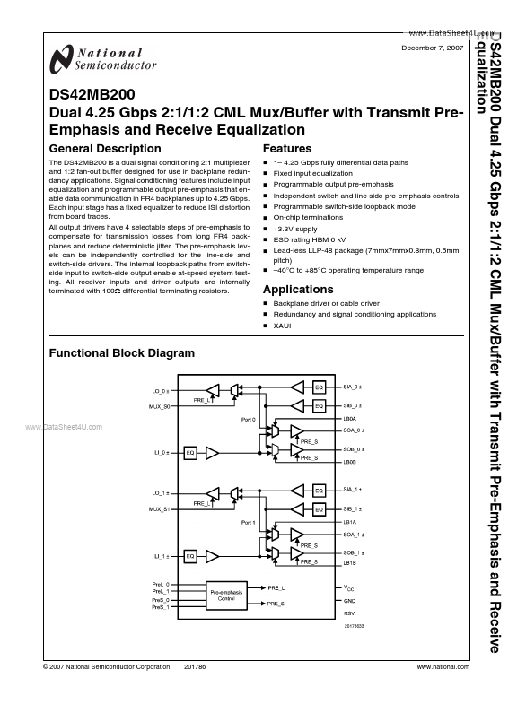
The DS42MB200 is a dual signal conditioning 2:1 multiplexer and 1:2 fan-out buffer designed for use in backplane redundancy applications. Signal conditioning features include input equalization and programmable output pre-emphasis that enable data munication in FR4 backplanes up to 4.25 Gbps. Each input stage has a fixed equalizer to reduce ISI distortion from board traces. All output drivers have 4 selectable steps of pre-emphasis to pensate for transmission losses from long FR4 backplanes and reduce deterministic jitter. The pre-emphasis levels can be independently controlled for the line-side and switch-side drivers. The internal loopback paths from switchside input to switch-side output enable at-speed system testing. All receiver inputs and driver outputs are internally terminated with 100Ω differential terminating resistors.
Features
- -
- -
- -
- -
- 1- 4.25 Gbps fully differential data paths Fixed input equalization Programmable output pre-emphasis Independent switch and line side pre-emphasis controls Programmable switch-side loopback mode On-chip terminations +3.3V supply ESD rating HBM 6 k V Lead-less LLP-48 package (7mmx7mmx0.8mm, 0.5mm pitch)
- - 40°C to +85°C operating temperature range
Applications
- Backplane driver or cable driver
- Redundancy and signal conditioning applications
- XAUI
Functional Block Diagram
..
© 2007 National Semiconductor Corporation
.national.
Simplified Block Diagram
..
.national.
Connection Diagram
..
Order number DS42MB200TSQ See NS Package Number SQA48D
.national.
Pin Descriptions
Pin Name LI_0+ LI_0- LO_0+ LO_0- LI_1+ LI_1- LO_1+ LO_1- SOA_0+ SOA_0- SOB_0+ SOB_0- SIA_0+ SIA_0- SIB_0+ SIB_0- SOA_1+ SOA_1- SOB_1+ SOB_1- SIA_1+ SIA_1- SIB_1+ SIB_1- MUX_S0 MUX_S1 Pin Number 6 7 33 34 30 31 9 10 46 45 4 3 40 39 43 42 22 21 28 27 16 15 19 18 37 13 12 1 36 25 47 48 23 24 26 I I I/O I O I O Description
Inverting and non-inverting...