DS89C21
DS89C21 is Differential CMOS Line Driver and Receiver Pair manufactured by National Semiconductor.
Description
The DS89C21 is a differential CMOS line driver and receiver pair, designed to meet the requirements of TIA/EIA-422-A (RS-422) electrical characteristics interface standard. The DS89C21 provides one driver and one receiver in a minimum footprint. The device is offered in an 8-pin SOIC package. The CMOS design minimizes the supply current to 6 m A, making the device ideal for use in battery powered or power conscious applications. The driver features a fast transition time specified at 2.2 ns, and a maximum differential skew of 2 ns making the driver ideal for use in high speed applications operating above 10 MHz. The receiver can detect signals as low as 200 m V, and also incorporates hysteresis for noise rejection. Skew is specified at 4 ns maximum. The DS89C21 is patible with TTL and CMOS levels (DI and RO).
Features n Meets TIA/EIA-422-A (RS-422) and CCITT V.11 remendation n LOW POWER design
- 15 m W typical n Guaranteed AC parameters:
- Maximum driver skew 2.0 ns
- Maximum receiver skew 4.0 ns n Extended temperature range:
- 40˚C to +85˚C n Available in SOIC packaging n Operates over 20 Mbps n Receiver OPEN input failsafe feature
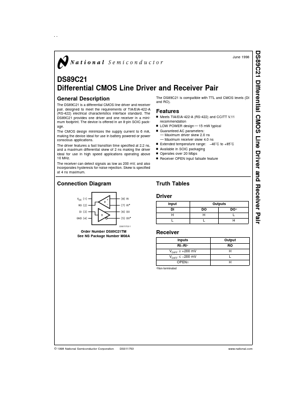
Connection Diagram
Truth Tables Driver
Input DI H L
DS011753-1
Outputs DO H L DO- L H
Order Number DS89C21TM See NS Package Number M08A
Receiver
Inputs RI- RI- VDIFF ≥ +200 m V VDIFF ≤
- 200 m V OPEN†
†Non-terminated
Output RO H L H
© 1998 National Semiconductor Corporation
DS011753
.national.
Absolute Maximum Ratings (Note 1)
If Military/Aerospace specified devices are required, please contact the National Semiconductor Sales Office/ Distributors for availability and specifications. Supply Voltage (VCC) Driver Input Voltage (DI) Driver Output Voltage (DO,
- DO ) Receiver Input Voltage
- V
7V
- 1.5V to VCC + 1.5V
- 0.5V to +7V
(TSTG)
- 65˚C to +150˚C +260˚C Lead Temperature (TL) (Soldering 4 sec.) Maximum Junction Temperature 150˚C Maximum Package Power Dissipation @+25˚C M Package 714 m W Derate M Package 5.7 m W/˚C...