DS90C401
DS90C401 is Dual Low Voltage Differential Signaling Driver manufactured by National Semiconductor.
Description
The DS90C401 is a dual driver device optimized for high data rate and low power applications. This device along with the DS90C402 provides a pair chip solution for a dual high speed point-to-point interface. The DS90C401 is a current mode driver allowing power dissipation to remain low even at high frequency. In addition, the short circuit fault current is also minimized. The device is in a 8 lead small outline package. The differential driver outputs provides low EMI with its low output swings typically 340 m V.
Features n n n n n Ultra low power dissipation Operates above 155.5 Mbps Standard TIA/EIA-644 8 Lead SOIC Package saves space Low Differential Output Swing typical 340 m V
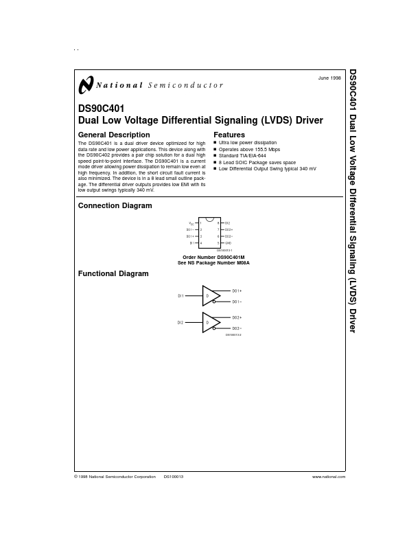
Connection Diagram
DS100013-1
Order Number DS90C401M See NS Package Number M08A
Functional Diagram
DS100013-2
© 1998 National Semiconductor Corporation
DS100013
.national.
Absolute Maximum Ratings (Note 1)
If Military/Aerospace specified devices are required, please contact the National Semiconductor Sales Office/ Distributors for availability and specifications. Supply Voltage (VCC)
- 0.3V to +6V
- 0.3V to (VCC + 0.3V) Input Voltage (DIN)
- 0.3V to (VCC + 0.3V) Output Voltage (DOUT+, DOUT- ) Short Circuit Duration Continuous (DOUT+, DOUT- ) Maximum Package Power Dissipation @ +25˚C M Package 1068 m W Derate M Package 8.5 m W/˚C above +25˚C Storage Temperature Range
- 65˚C to +150˚C Lead Temperature Range Soldering (4 sec.) +260˚C
Maximum Junction Temperature ESD Rating (HBM, 1.5 kΩ, 100 p F) (EIAJ, 0 Ω, 200 p F)
+150˚C ≥ 3,500V ≥ 250V
Remended Operating Conditions
Supply Voltage (VCC) Operating Free Air Temperature (TA) Min +4.5
- 40 Typ +5.0 +25 Max +5.5 +85 Units V ˚C
Electrical Characteristics
Over supply voltage and operating temperature ranges, unless otherwise specified. (Notes 2, 3) Symbol VOD1 ∆VOD1 Parameter Differential Output Voltage Change in Magnitude of VOD1 for plementary Output States Offset Voltage Change in Magnitude of VOS for plementary Output States...