DS90LV027
DS90LV027 is LVDS Dual High Speed Differential Driver manufactured by National Semiconductor.
Description
The DS90LV027 is a dual LVDS driver device optimized for high data rate and low power applications. The DS90LV027 is a current mode driver allowing power dissipation to remain low even at high frequency. In addition, the short circuit fault current is also minimized. The device is in a 8-lead small Outline Package. The DS90LV027 has a flow-through design for easy PCB layout. The differential driver outputs provides low EMI with its low output swings typically 340 m V. Perfect for high speed transfer of clock and data. Pair with any of National’s LVDS receivers.
Features n n n n n n n n Ultra Low Power Dissipation Operating Range above 155 Mbps Flow-through pinout simplifies PCB layout Conforms to TIA/EIA-644 Standard 8-Lead SOIC Package Saves Space VCM ± 1V center around 1.2V Low Differential Output Swing Typical 340 m V Power Off Protection (outputs in high impedance)
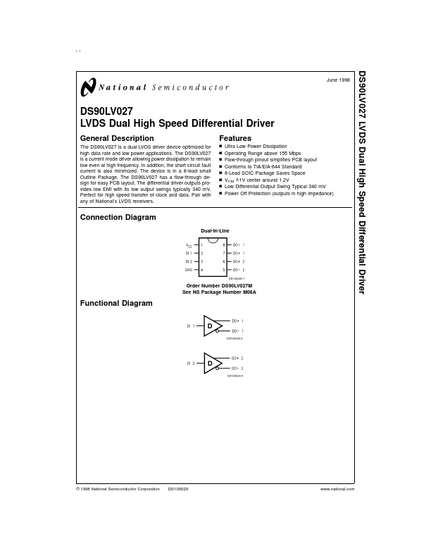
Connection Diagram
Dual-In-Line
DS100029-1
Order Number DS90LV027M See NS Package Number M08A
Functional Diagram
DS100029-2
DS100029-3
© 1998 National Semiconductor Corporation
DS100029
.national.
Absolute Maximum Ratings (Note 1)
If Military/Aerospace specified devices are required, please contact the National Semiconductor Sales Office/ Distributors for availability and specifications. Supply Voltage (VCC)
- 0.3V to +6V Input Voltage (DI)
- 0.3V to (VCC + 0.3V)
- 0.3V to +3.9V Output Voltage (DO ± ) Maximum Package Power Dissipation @ +25˚C M Package 1190 m W Derate M Package 9.5 m W/˚C above +25˚C Storage Temperature Range
- 65˚C to +150˚C
Lead Temperature Range Soldering (4 sec.) ESD Rating (Note 4) (HBM 1.5 kΩ, 100 p F)
+260˚C ≥ 4.5 k V
Remended Operating Conditions
Supply Voltage (VCC) Temperature (TA) Min 3.0 0 Typ 3.3 25 Max 3.6 70 Units V ˚C
Electrical Characteristics
Over Supply Voltage and Operating Temperature ranges, unless otherwise specified. (Notes 2, 3, 7) Symbol Parameter Conditions Pin DO+, DO- Min 250 0 0.9 0.9 0 VOUT = VCC or GND VOUT = 3.6V or GND, VCC = 0V DI...