DS90LV028AH
DS90LV028AH is High Temperature 3V LVDS Dual Differential Line Receiver manufactured by National Semiconductor.
Description
The DS90LV028AH is a dual CMOS differential line receiver designed for applications requiring ultra low power dissipation, low noise and high data rates. The device is designed to support data rates in excess of 400 Mbps (200 MHz) utilizing Low Voltage Differential Signaling (LVDS) technology. The DS90LV028AH accepts low voltage (350 m V typical) differential input signals and translates them to 3V CMOS output levels. The DS90LV028AH has a flow-through design for easy PCB layout. The DS90LV028AH and panion LVDS line driver DS90LV027AH provide a new alternative to high power PECL/ECL devices for high speed point-to-point interface applications.
Features n n n n n n n n n n n n -40˚C to +125˚C operating temperature range > 400 Mbps (200 MHz) switching rates 50 ps differential skew (typical) 0.1 ns channel-to-channel skew (typical) 2.5 ns maximum propagation delay 3.3V power supply design Flow-through pinout Power down high impedance on LVDS inputs Low Power design (18m W @ 3.3V static) LVDS inputs accept LVDS/CML/LVPECL signals Conforms to ANSI/TIA/EIA-644 Standard Available in SOIC package
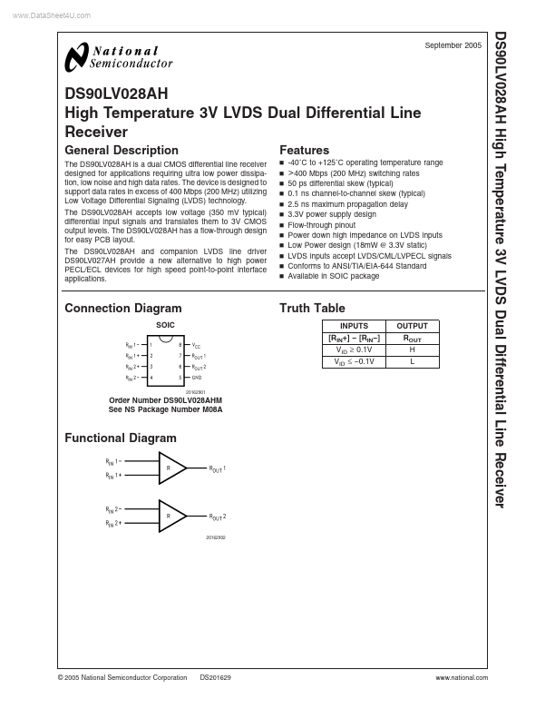
Connection Diagram
SOIC
Truth Table
INPUTS [RIN+]
- [RIN- ] VID ≥ 0.1V VID ≤
- 0.1V OUTPUT ROUT H L
Order Number DS90LV028AHM See NS Package Number M08A
Functional Diagram
© 2005 National Semiconductor Corporation
DS201629
.national.
Absolute Maximum Ratings (Note 1)
If Military/Aerospace specified devices are required, please contact the National Semiconductor Sales Office/ Distributors for availability and specifications. Supply Voltage (VCC) Input Voltage (RIN+, RIN- ) Output Voltage (ROUT) M Package Derate M Package Storage Temperature Range Lead Temperature Range Soldering (4 sec.) +260˚C
- 0.3V to +4V
- 0.3V to +3.9V
- 0.3V to VCC + 0.3V 1025 m W 8.2 m W/˚C above +25˚C
- 65˚C to +150˚C
Maximum Junction Temperature ESD Rating (Note 4) (HBM 1.5 kΩ, 100 p F) (EIAJ 0Ω, 200 p F)
+150˚C ≥ 7 k V ≥ 500 V
Maximum Package Power Dissipation @...