DS9643
DS9643 is Dual TTL to MOS/CCD Driver manufactured by National Semiconductor.
Description
The DS9643 is a dual positive logic ‘‘AND’’ TTL-to-MOS driver The DS9643 is a functional replacement for the SN75322 with one important exception the two external PNP transistors are no longer needed for operation The DS9643 is also a functional replacement for the 75363 with the important exception that the VCC3 supply is not needed The lead connections normally used for the external PNP transistors are purposely not internally connected to the DS9643
Features
Y Satisfies CCD memory and delay line requirements Y Dual positive logic TTL to MOS driver Y Operates from standard bipolar and MOS supply volt- ages Y High speed switching Y TTL and DTL patible inputs Y Separate drivers address inputs with mon strobe Y VOH and VOL patible with popular MOS RAMs Y Does not require external PNP transistors or VCC3 Y VOH minimum is VCC2 b 0 5V
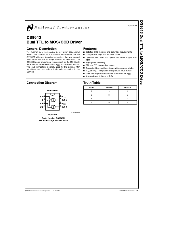
Connection Diagram
8-Lead DIP
Truth Table
Input L L H H
Enable L H L H
Output L L L H
Top View
Order Number DS9643N See NS Package Number N08E
TL F 9646
- 1
C1995 National Semiconductor Corporation TL F 9646
RRD-B30M115 Printed in U S A
Absolute Maximum Ratings (Note 1)
If Military Aerospace specified devices are required please contact the National Semiconductor Sales Office Distributors for availability and specifications
Storage Temperature Range b65 C to a150 C
Operating Temperature Range
0 C to a70 C
Lead Temperature Molded DIP (soldering 10 sec )
265 C
Maximum Power Dissipation at 25 C Molded Package
930 m W
Supply Voltage Range of VCC1 Range of VCC2
Input Voltage b0 5V to a7 0V b0 5V to a15V
5 5V
Derate molded DIP package 7 5 m W C above 25 C
Remended Operating
Conditions
Min Typ Max Units
Supply Voltage (VCC1)
4 75 5 0 5 25 V
Supply Voltage (VCC2)
11 4 12 12 6 V
Operating Temperature (TA) 0
25 70
Electrical Characteristics over remended operating temperatures and VCC1 VCC2 ranges unless otherwise specified (Notes 2 and...