DS99R104
DS99R104 is DC-Balanced 24-Bit LVDS Serializer and Deserializer manufactured by National Semiconductor.
- Part of the DS99R103 comparator family.
- Part of the DS99R103 comparator family.
Description
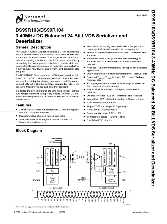
The DS99R103/104 Chipset translates a 24-bit parallel bus into a fully transparent data/control LVDS serial stream with embedded clock information. This single serial stream simplifies transferring a 24-bit bus over PCB traces and cable by eliminating the skew problems between parallel data and clock paths. It saves system cost by narrowing data paths that in turn reduce PCB layers, cable width, and connector size and pins. The DS99R103/104 incorporates LVDS signaling on the highspeed I/O. LVDS provides a low power and low noise environment for reliably transferring data over a serial transmission path. By optimizing the serializer output edge rate for the operating frequency range EMI is further reduced. In addition the device features pre-emphasis to boost signals over longer distances using lossy cables. Internal DC balanced encoding/decoding is used to support AC-Coupled interconnects.
- Internal DC Balancing encode/decode
- Supports AC-
- -
- -
- -
- -
- -
- -
- -
Features
..
- 3 MHz- 40 MHz clock embedded and DC-Balancing 24:1 and 1:24 data transmissions
- Capable to drive shielded twisted-pair cable
- User selectable clock edge for parallel data on both
Transmitter and Receiver coupling interface with no external coding required Individual power-down controls for both Transmitter and Receiver Embedded clock CDR (clock and data recovery) on Receiver and no external source of reference clock needed All codes RDL (random data lock) to support hot-pluggable applications LOCK output flag to ensure data integrity at Receiver side Balanced TSETUP/THOLD between RCLK and RDATA on Receiver side PTO (progressive turn-on) LVCMOS outputs to reduce EMI and minimize SSO effects All LVCMOS inputs and control pins have internal pulldown On-chip filters for PLLs on Transmitter and Receiver Integrated 100Ω (±20%) termination in Receiver input 4 m A Receiver output drive 48-pin TQFP and 48-pin LLP packages Pure CMOS .35 μm process Power supply range 3.3V ± 10%...