LF453
LF453 is LF453 Wide-Bandwidth Dual JFET-Input Operational Amplifiers manufactured by National Semiconductor.
Description
The LF453 is a low-cost high-speed dual JFET-input operational amplifier with an internally trimmed input offset voltage (BI-FET II technology) The device requires a low supply current and yet the amplifiers maintain a large gain bandwidth product and a fast slew rate In addition well matched high voltage JFET input devices provide very low input bias and offset currents The LF453 is pin patible with the standard LM1558 allowing designers to upgrade the overall performance of existing designs The LF453 may be used in such applications as high-speed integrators fast D A converters sample-and-hold circuits and many other circuits requiring low input bias current high input impedance high slew rate and wide bandwidth
Features
Y Y Y Y Y Y Y Y
Internally trimmed offset voltage Low input bias current Low input noise current Wide gain bandwidth High slew rate Low supply current High input impedance Low total harmonic distortion AV e 10 RL e 10k VO e 20 Vp- p f e 20 Hz
- 20 k Hz Low 1 f noise corner Fast settling time to 0 01%
5 0 m V (max) 50 p A (typ) 0 01 p A SHz (typ) 4 MHz (typ) 13 V ms (typ) 6 5 m A (max) 1012X (typ) k 0 02% (typ)
50 Hz (typ) 2 ms (typ)
Typical Connection
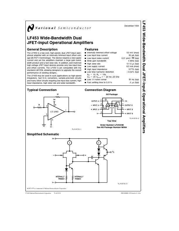
Connection Diagram
SO Package
TL H 9710
- 2
Top View Order Number LF453CM See NS Package Number M08A
TL H 9710
- 1
Simplified Schematic
TL H 9710
- 3
BI-FET IITM is a trademark of National Semiconductor Corporation
C1995 National Semiconductor Corporation
TL H 9710
RRD-B30M115 Printed in U S A
Absolute Maximum Ratings (Note 1) If Military Aerospace specified devices are required please contact the National Semiconductor Sales Office Distributors for availability and specifications
Supply Voltage (V a b Vb) Input Voltage Range Differential Input Voltage (Note 2) Junction Temperature (TJ MAX) Output Short Circuit Duration Power Dissipation (Note 3) ESD Tolerance 36V Vb s VIN s V a g 30V 150 C Continuous 500 m W TBD
Soldering Information (Note 4) SO Package Vapor Phase (60 sec...