LM1296
LM1296 is Raster Geometry Correction System manufactured by National Semiconductor.
Description
The LM1296 is a monolithic IC for use in the raster scanning circuitry of a multi-frequency CRT monitor. The IC provides an S-corrected sawtooth waveform and a variable DC output voltage. These two outputs drive the vertical deflection amplifier. It also provides another waveform for East-West geometry correction which includes pincushion, corner, and trapezoid controls. The geometry correction is controlled by DC input voltages from 0V to 4V. The raster height and the raster vertical position can be controlled by two DC voltage input pins that adjust the sawtooth waveform amplitude and the variable DC output voltage. The East-West correction of the LM1296 has height tracking and vertical position tracking capabilities. As the height or position of the raster is adjusted the geometry correction is maintained by the chip automatically. The LM1296 is packaged in a 16-pin plastic DIP package. Accepts either polarity of V sync DC-controlled correction terms Raster vertical position control Vertical S-correction (linearity) control East-West pincushion control East-West trapezoid control East-West corner control Provides both polarities of correction output East-West correction tracks raster vertical position and height n patible with LM1290 and LM1292 horizontal PLL n n n n n n n n n
Applications n Vertical deflection of monitors
Features n Vertical scanning frequency 50 Hz- 165 Hz
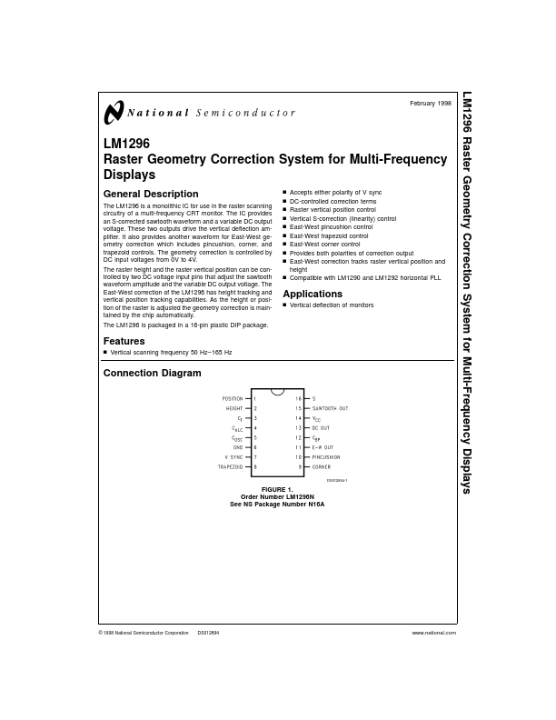
Connection Diagram
DS012894-1
FIGURE 1. Order Number LM1296N See NS Package Number N16A
© 1998 National Semiconductor Corporation
DS012894
.national.
Absolute Maximum Ratings (Notes 3, 1)
If Military/Aerospace specified devices are required, please contact the National Semiconductor Sales Office/ Distributors for availability and specifications. Supply Voltage (VCC) Input Voltage (VIN) Pins 1, 2, 8, 9, 10, 16 Power Dissipation (PD) Above 25˚C, Derate Based on θJA and TJ (Note 4) Thermal Resistance (θJA) Junction Temperature (TJMAX) 15V 0V ≤ VIN ≤ 5V
ESD Susceptibility...