LMK02000
LMK02000 is Precision Clock Conditioner manufactured by National Semiconductor.
Description
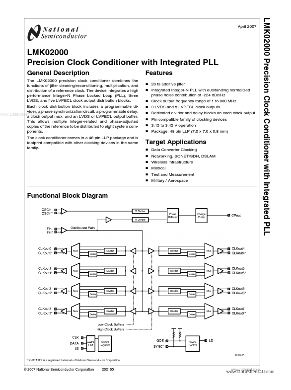
The LMK02000 precision clock conditioner bines the functions of jitter cleaning/reconditioning, multiplication, and distribution of a reference clock. The device integrates a high performance Integer-N Phase Locked Loop (PLL), three LVDS, and five LVPECL clock output distribution blocks. Each clock distribution block includes a programmable divider, a phase synchronization circuit, a programmable delay, .. a clock output mux, and an LVDS or LVPECL output buffer. This allows multiple integer-related and phase-adjusted copies of the reference to be distributed to eight system ponents. The clock conditioner es in a 48-pin LLP package and is footprint patible with other clocking devices in the same family.
Features
- 20 fs additive jitter
- Integrated Integer-N PLL with outstanding normalized
- -
- -
- - phase noise contribution of -224 d Bc/Hz Clock output frequency range of 1 to 800 MHz 3 LVDS and 5 LVPECL clock outputs Dedicated divider and delay blocks on each clock output Pin patible family of clocking devices 3.15 to 3.45 V operation Package: 48 pin LLP (7.0 x 7.0 x 0.8 mm)
Target Applications
- -
- -
- -
Data Converter Clocking Networking, SONET/SDH, DSLAM Wireless Infrastructure Medical Test and Measurement Military / Aerospace
Functional Block Diagram
TRI-STATE® is a registered trademark of National Semiconductor Corporation.
© 2007 National Semiconductor Corporation
.national.
Connection Diagram
48-Pin LLP Package
..
.national.
Pin Descriptions
Pin # 1, 25 2, 7 Pin Name GND NC I/O I I I I O O O O O I I O I I O O O O Ground No Connection to these pins Power Supply MICROWIRE Clock Input MICROWIRE Data Input MICROWIRE Latch Enable Input LDO Bypass Global Output Enable Lock Detect and Test Output LVDS Clock Output 0 LVDS Clock Output 1 LVDS Clock Output 2 LVPECL Clock Output 3 Global Clock Output Synchronization Oscillator Clock Input; Must be AC coupled Charge Pump Output Frequency Input;...